Active element, pixel structure and display panel

A pixel structure and active component technology, applied in electrical components, electric solid-state devices, semiconductor devices, etc., can solve the problems of power consumption, increase the display panel, increase the load of pixel structure, etc., and achieve the effect of high aperture ratio

Inactive Publication Date: 2011-05-18
AU OPTRONICS CORP
View PDF0 Cites 20 Cited by
  • Summary
  • Abstract
  • Description
  • Claims
  • Application Information

AI Technical Summary

Problems solved by technology

However, since the overlapping of the capacitive electrode and the data line will increase the loading of the pixel structure, such a pixel structure will increase the power required for driving the display panel and consume more power.

Method used


Image

  • Active element, pixel structure and display panel
  • Active element, pixel structure and display panel
  • Active element, pixel structure and display panel

Examples


Embodiment Construction

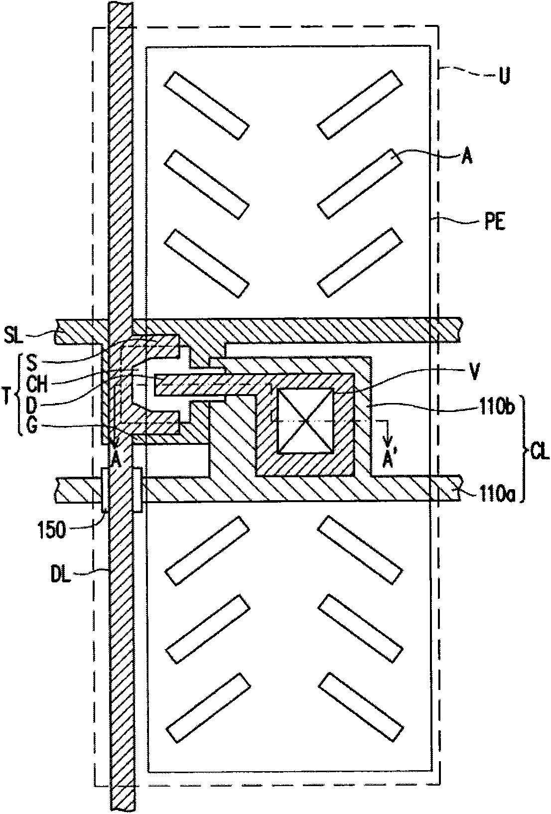
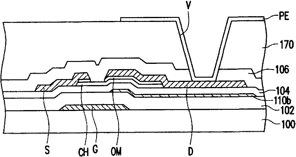
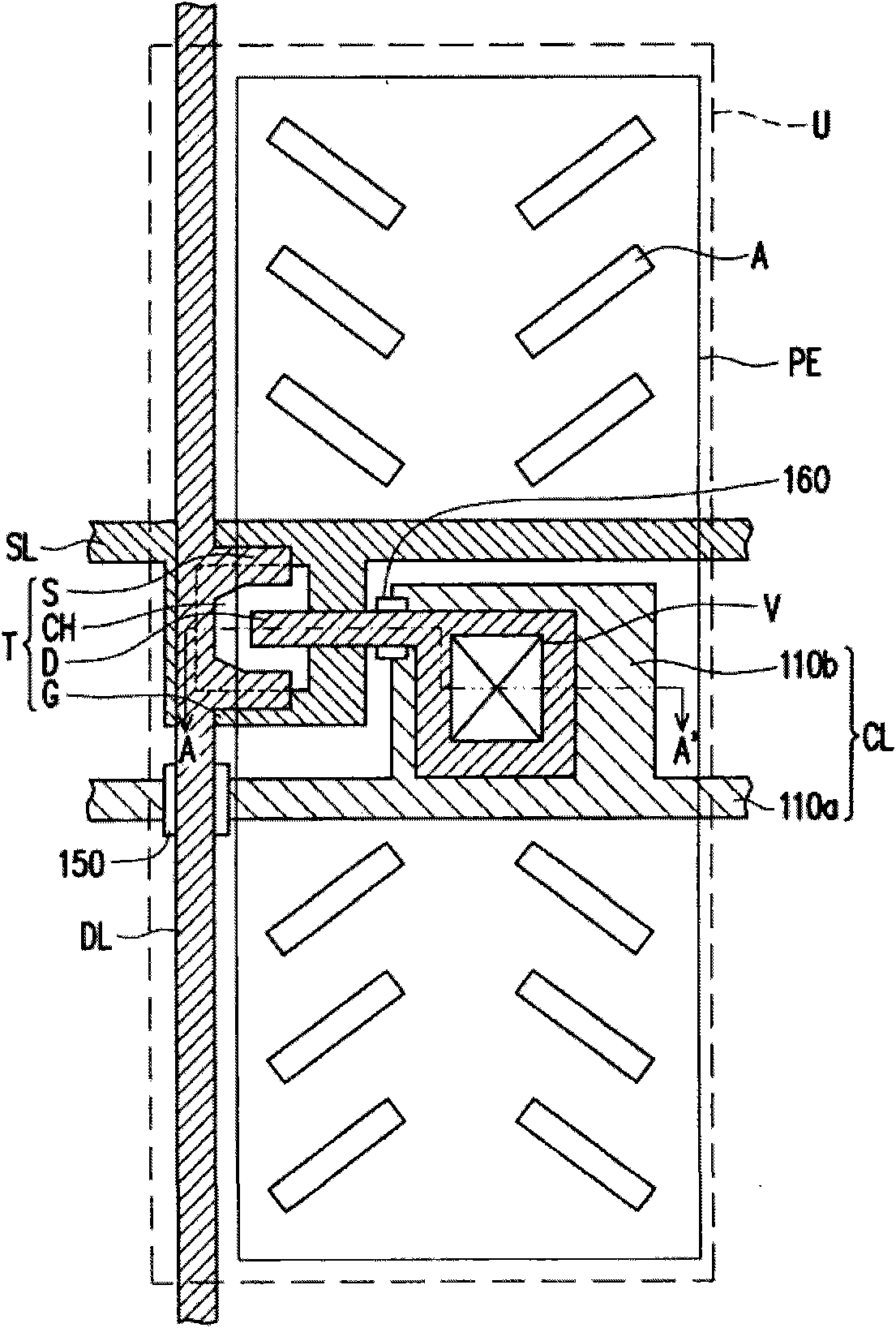
[0049] Figure 1A is a schematic top view of a pixel structure according to an embodiment of the present invention. Figure 1B yes Figure 1A Schematic cross-section along section line A-A'. Please also refer to Figure 1A as well as Figure 1B The pixel structure of this embodiment includes scan lines SL, data lines DL, active elements T, gate insulating layers 102 / 104 , pixel electrodes PE, capacitor electrodes CL and capacitor dielectric layers 104 disposed on the substrate 100 .

[0050] The substrate 100 has a pixel area U, and one pixel structure is disposed in one pixel area U. The material of the substrate 100 can be glass, quartz, organic polymer, or opaque / reflective material (eg, conductive material, chip, ceramic, or other applicable materials), or other applicable materials. The scan lines SL and the data lines DL are disposed on the substrate 100 .

[0051] The scan lines SL and the data lines DL are arranged to cross over each other. In other words, the ex...


PUM

PropertyMeasurementUnit
thicknessaaaaaaaaaa
thicknessaaaaaaaaaa

Abstract

The invention provides an active element, a pixel structure and a display panel. The pixel structure comprises a scanning line, a data line, an active element, grid electrode insulating layers, a pixel electrode, a capacitance electrode and a capacitance dielectric layer, wherein the active element comprises a grid electrode, a channel, a source electrode and a drain electrode; the scanning line is electrically connected with the grid electrode; the source electrode is electrically connected with the data line; the grid electrode insulating layers are arranged between the grid electrode and the channel; the pixel electrode is electrically connected with the drain electrode; the capacitance electrode is positioned on the grid electrode insulating layers and/or between the grid electrode insulating layers; and the capacitance dielectric layer is positioned between the capacitance electrode and the drain electrode.

Description

technical field [0001] The invention relates to an active element, a pixel structure and a display panel with the active element. Background technique [0002] Generally speaking, a pixel structure of a liquid crystal display includes an active element and a pixel electrode. The active element is used as the switching element of the liquid crystal display unit. In order to control individual pixel structures, a specific pixel is usually selected through corresponding scan lines and data lines, and an appropriate operating voltage is provided to display display data corresponding to the pixel. In addition, the pixel structure also includes a storage capacitor (storage capacitor), so that the pixel structure has a voltage holding function. That is, the storage capacitor can store the above-mentioned applied operating voltage to maintain the stability of the display picture of the pixel structure. [0003] In order to provide storage capacitors in the pixel structure, it is ...

Claims


Application Information

Patent Timeline
Patent Type & Authority Applications(China)
IPC IPC(8): H01L27/12H01L29/41G02F1/1362G02F1/1368
Inventor 陈昱丞李怡慧林志宏陈茂松
Owner AU OPTRONICS CORP
Why Eureka
Try Eureka