Optical sheet, light-emitting device, and method for manufacturing optical sheet

A light-emitting device and manufacturing method technology, applied in the direction of electroluminescence light source, optics, optical components, etc., can solve the problems of raising the cost of the product, failing to guarantee the light extraction efficiency, exceeding the critical angle, etc., achieving a simple structure and suppressing the light intensity The distribution and color imbalance, the effect of improving the light extraction efficiency

Inactive Publication Date: 2011-05-18
PANASONIC CORP
View PDF9 Cites 6 Cited by
  • Summary
  • Abstract
  • Description
  • Claims
  • Application Information

AI Technical Summary

Problems solved by technology

[0021] In addition, in the technology disclosed in Patent Document 1, although it is possible to extract light that will become total reflection with certainty, the opposite also exists.
That is, when it is assumed that there is no diffraction grating layer, the light emitted from a point in the light-emitting layer may be incident at an angle smaller than the critical angle on the refracting surface (exiting surface) of the transparent substrate and be transmitted and refracted. When there is a diffraction grating layer and diffraction occurs due to this, the incident angle on the refracting surface exceeds the critical angle and total reflection occurs.
Therefore, the technology disclosed in Patent Document 1 cannot guarantee improvement in light extraction efficiency.
In addition, in the technique disclosed in Patent Document 1, diffracted light in which all light rays uniformly move in a predetermined direction occurs.
Light including such diffracted light has a distribution of light intensity due to azimuth, and since a predetermined amount of movement depends on the wavelength of outgoing light, there is an imbalance of color due to azimuth.
[0022] In addition, in the light-emitting device disclosed in Patent Document 1, light incident from the outside (air layer side) is regularly reflected by the surface of the transparent substrate, and constitutes interference (so-called reflection) with respect to light extracted from the light-emitting layer. Optical treatment such as an anti-reflection film is required on the surface of the transparent substrate, which increases the cost of the product
[0023] On the other hand, the purpose of the light-emitting device disclosed in Patent Document 2 is to prevent the reflection of light on the refracting surface, and the improvement in light extraction efficiency brought about by this structure is very small, only about 10 to 20 percent.

Method used


Image

  • Optical sheet, light-emitting device, and method for manufacturing optical sheet
  • Optical sheet, light-emitting device, and method for manufacturing optical sheet
  • Optical sheet, light-emitting device, and method for manufacturing optical sheet

Examples


no. 1 approach

[0102] based on Figures 12-19 , Figure 27 , to describe the first embodiment.

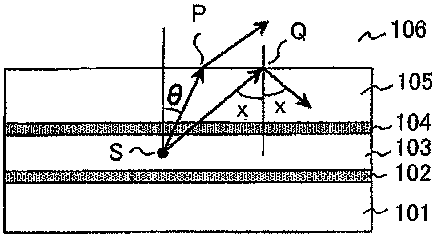
[0103] Figure 12 The cross-sectional structure and light propagation of the light emitting device using the organic EL element in the first embodiment are shown. An electrode 2 , a light emitting layer 3 , and a transparent electrode 4 are stacked in this order on a substrate 1 , and a transparent substrate (transparent protective layer) 5 is formed on the transparent electrode 4 . The substrate 1, the electrode 2, the light-emitting layer 3, and the transparent electrode 4 constitute a luminous body. On the surface of the transparent substrate 5 is formed a surface structure 13 divided into minute domains and having fine unevenness.

[0104] A voltage is applied between the electrode 2 and the transparent electrode 4, and the point S inside the light-emitting layer 3 emits light. The light passes through the transparent electrode 4 directly or after being reflected by the electrode 2, and i...

no. 2 approach

[0135] based on Figure 22 , Figure 23 A second embodiment will be described. In the second embodiment, only the pattern of the surface structure 13 is different from the first embodiment, and the other structures are completely the same as those of the first embodiment, and descriptions of the common structures are omitted.

[0136] In the second embodiment, the convex ratio P and the concave ratio 1-P of the surface structure are not fixed at 0.5, but are set at P=0.4 to 0.98. That is, the micro-region δ 1 (Area protruding upward) exists 40-98%, micro-region δ 2 (Concavity) exists in 60-2%.

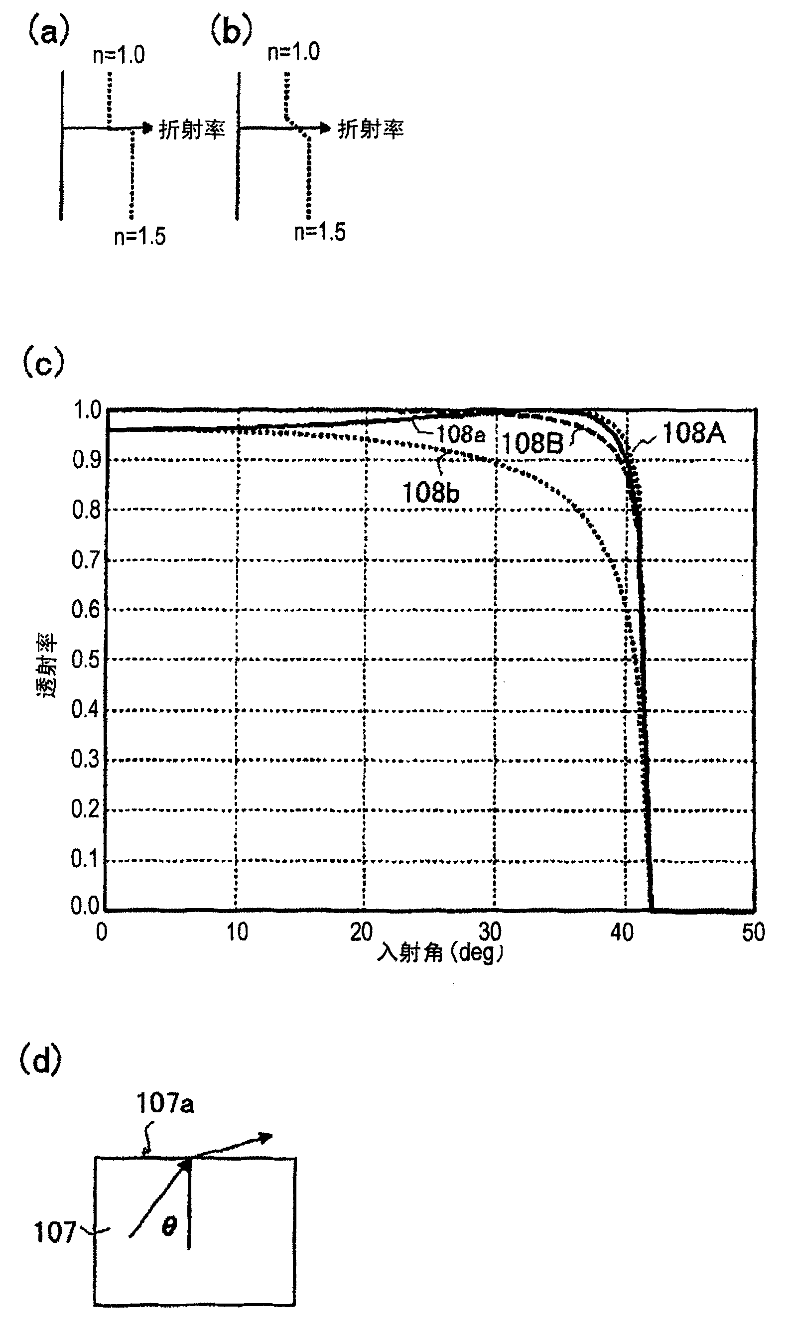
[0137] Figure 22 (a) is a graph explaining the light extraction efficiency of the surface structure of this embodiment, showing the refractive index n of the transparent substrate 5 1 =1.457, the refractive index n of air 6 0 = 1.0, the wavelength λ of light = 0.635 μm, the protrusion height of the surface structure d = 0.70 μm, the horizontal axis is the boundary width w of th...

no. 3 approach

[0142] based on Figure 22 (b) The third embodiment will be described. In the third embodiment, only the height difference condition of the surface structure 13 is different, and other structures are completely the same as those of the first and second embodiments, and descriptions of common structures are omitted.

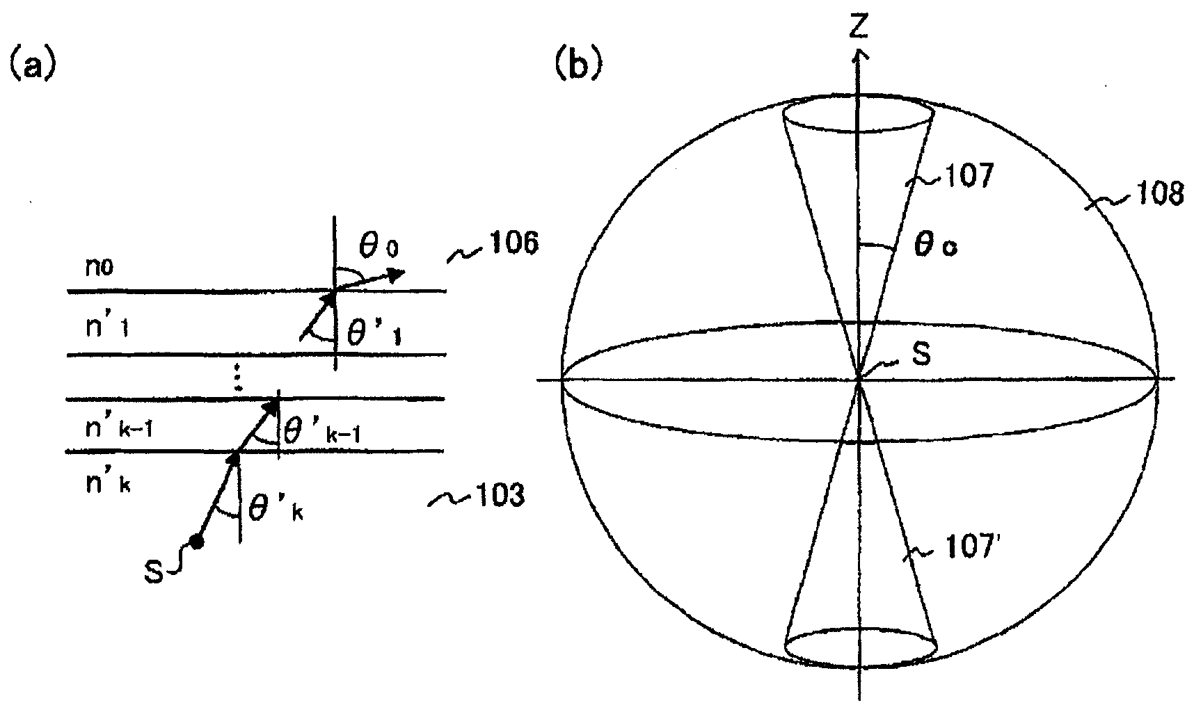
[0143] In the third embodiment, two adjacent minute regions δ of the surface structure in the first and second embodiments are 1 ,δ 2 The amount of height difference between randomizes the case. As a way to achieve randomness, in Figure 13 In (a), the surface of the transparent substrate 5 is divided into checkerboard grids (small square regions δ) of width w (referred to as the boundary width) without gaps, and random function is used in each grid with respect to a single reference plane. set-d m / 2~d m / 2 between any height (or depth). As a single reference plane, in the direction parallel to the surface normal of the surface of the transparent substrate...


PUM

PropertyMeasurementUnit
refractive indexaaaaaaaaaa
depthaaaaaaaaaa
widthaaaaaaaaaa

Abstract

A light-emitting device has a surface structure (13) of the surface of a transparent substrate (5). The surface structure is so configured that the surface of the transparent substrate (5) adjoining a light-emitting body is demarcated by multiple line segments having a width of approximate w inclined in a specific direction parallel to the surface, the line segments are divided in the length direction of the line segments by micro-regions such that the diameter of the largest one of the circles inscribing the micro-regions lies in the range from 0.2 [mu]m to 1.5 [mu]m, each of the micro-regions has a protruded or recessed shape on the surface of the transparent substrate (5), the proportions of the protrusions and recesses are P and 1-P respectively, and P lies in the range from 0.4 to 0.98.

Description

technical field [0001] The present invention relates to a transparent optical sheet, a light-emitting device, and a manufacturing method thereof, which are used so that one surface thereof adjoins a light-emitting body. Background technique [0002] As conventional techniques, there are techniques disclosed in Patent Documents 1 and 2, for example. [0003] figure 1 Shows the cross-sectional structure and propagation of light of a light-emitting device using a general organic electroluminescence element (organic EL element). On the substrate 101 , an electrode 102 , a light emitting layer 103 , and a transparent electrode 104 are stacked in this order, and a transparent substrate 105 is placed on the transparent electrode 104 . A voltage is applied between the electrode 102 and the transparent electrode 104, and the point S inside the light-emitting layer 103 emits light. The light passes through the electrode 104 directly or after being reflected by the electrode 102, and...

Claims


Application Information

Patent Timeline
Patent Type & Authority Applications(China)
IPC IPC(8): G02B5/00B32B3/30B32B7/02G02B5/02H01L51/50H05B33/02
CPCH01L51/5275G02B6/0003G02B5/02Y10T428/162H10K50/858
Inventor 若林信一西胁青儿铃木正明松崎纯平中村达也
Owner PANASONIC CORP
Why Eureka
Try Eureka