Semiconductor device and lead frame thereof

A semiconductor and lead frame technology, applied in the direction of semiconductor devices, semiconductor/solid-state device components, electric solid-state devices, etc., can solve problems such as difficult to improve withstand voltage, and achieve high withstand voltage

Inactive Publication Date: 2011-05-25
PANASONIC CORP
View PDF4 Cites 7 Cited by
  • Summary
  • Abstract
  • Description
  • Claims
  • Application Information

AI Technical Summary

Problems solved by technology

In conventional semiconductor devices, the distance between lead terminals is limited, so it is difficult to increase the withstand voltage

Method used


Image

  • Semiconductor device and lead frame thereof
  • Semiconductor device and lead frame thereof
  • Semiconductor device and lead frame thereof

Examples


Embodiment Construction

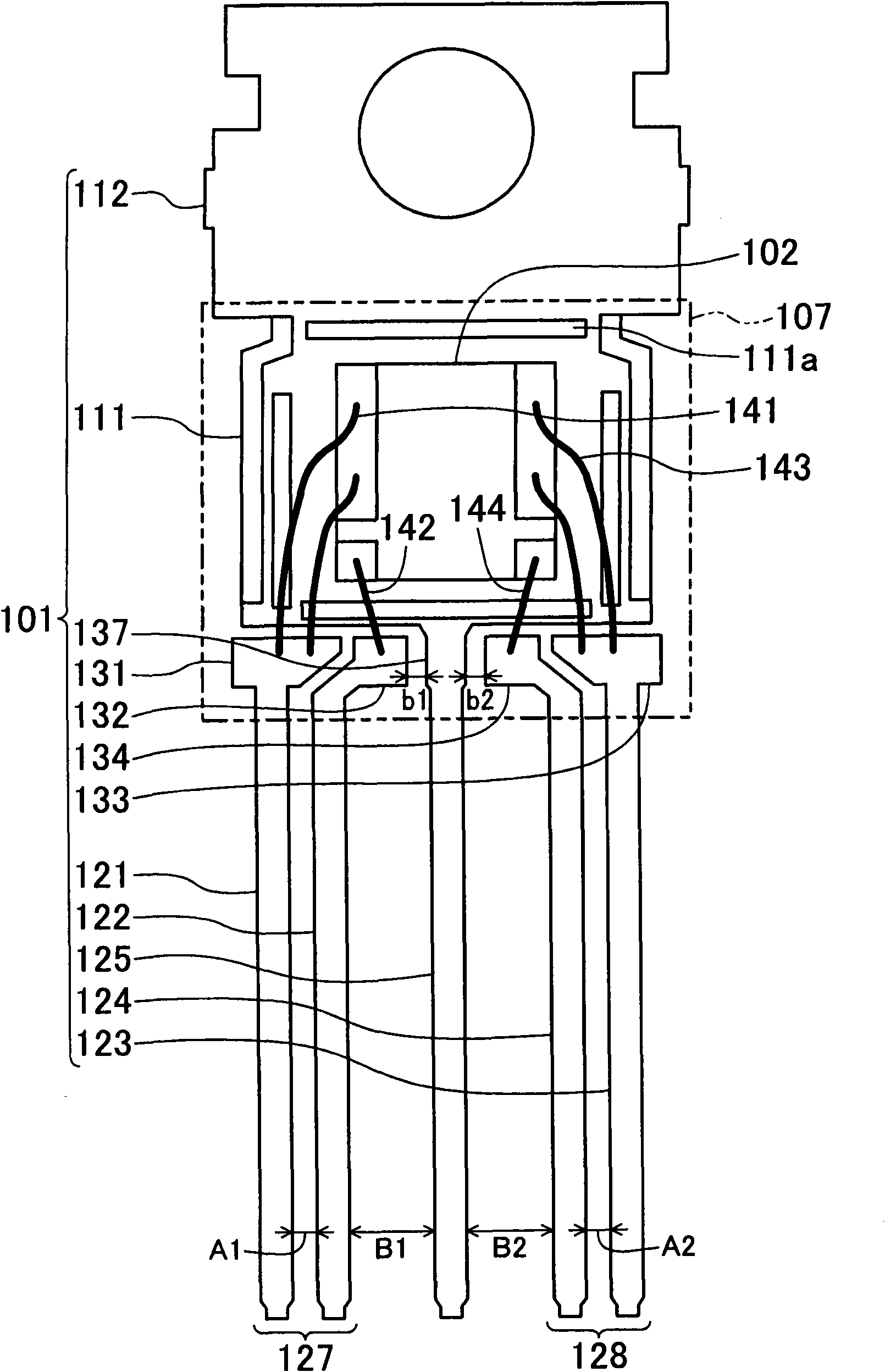
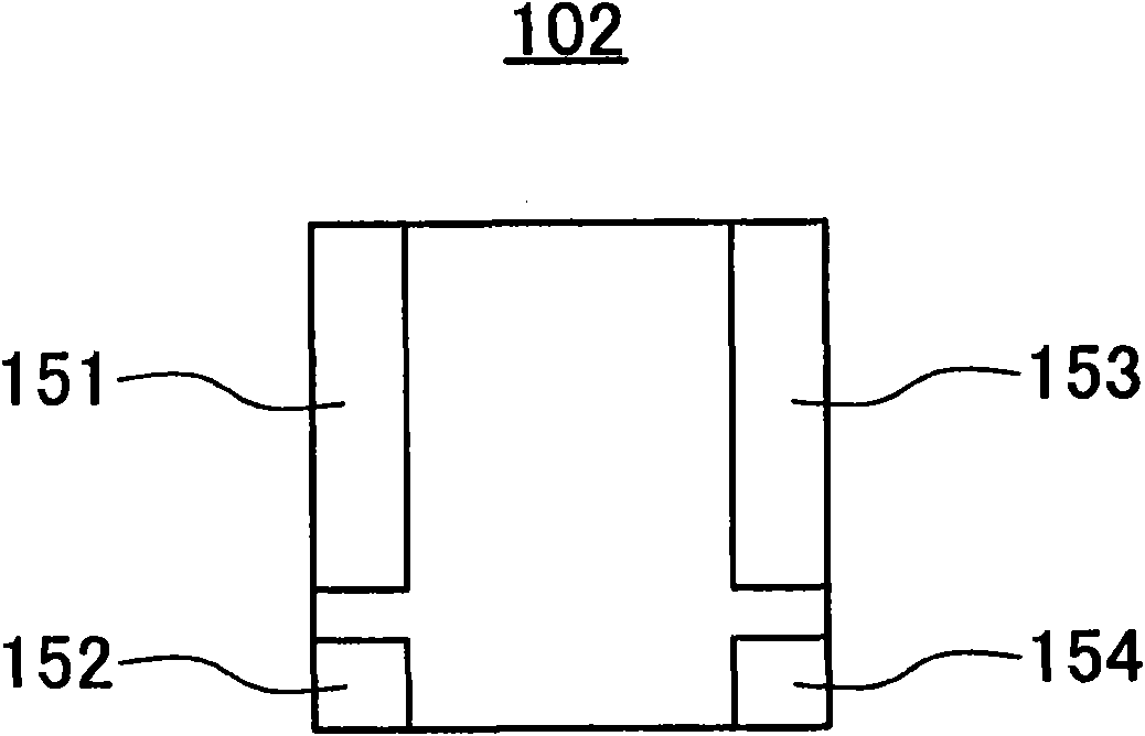
[0086] figure 1 A plan view structure of a semiconductor device according to an embodiment is shown. Such as figure 1 As shown in FIG. 2 , a semiconductor element 102 is mounted on a lead frame 101 and sealed by an insulating sealing portion 107 made of resin. and, in figure 1 Only the position of the insulating seal 107 is shown in .

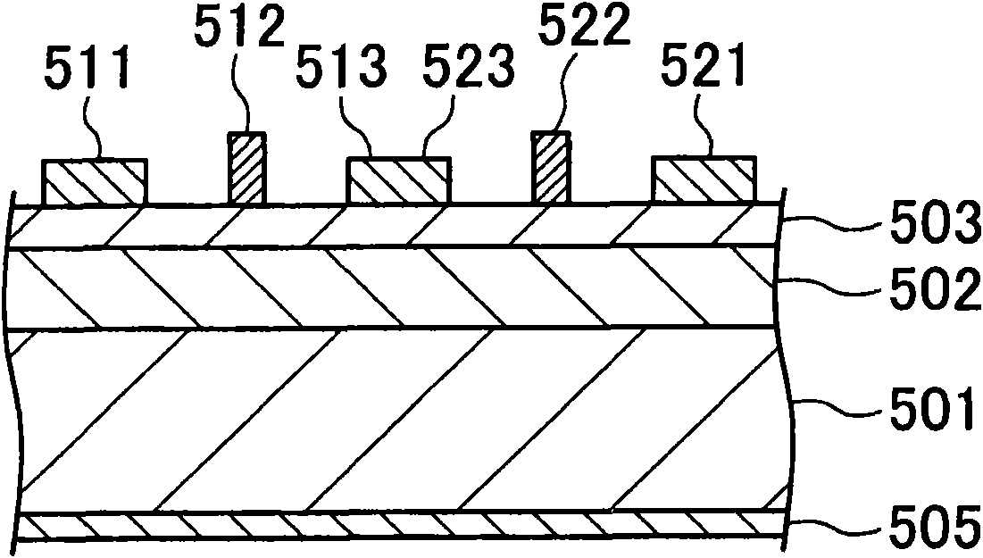
[0087] The semiconductor element 102 is, for example, a switching element for electric power or the like. If a specific example is given, it is as follows figure 2 Two field effect transistors (FETs) made of nitride semiconductors are integrally formed on a substrate as shown. A first nitride semiconductor layer 502 serving as a channel layer and a second nitride semiconductor layer 503 serving as an electron supply layer are sequentially formed over a substrate 501 . The first nitride semiconductor layer 502 may be, for example, gallium nitride (GaN), and the second nitride semiconductor layer 503 may be, for example, aluminum galliu...


PUM


Abstract

An objective of the present invention is to implement a small-sized semiconductor device that satisfies clearances required to secure the dielectric strength and allows flow of a large current. The semiconductor device includes a semiconductor element (102) and a lead frame (101). The lead frame (101) includes a first lead (121), a second lead (122), a third lead (123), a fourth lead (124), and a fifth lead (125) placed parallel to one another. The first and second leads are placed adjoining to each other and constitute a first lead group(127), and the third and fourth leads are placed adjoining to each other and constitute a second lead group(128). The spacing between the first lead group and the fifth lead, the spacing between the second lead group and the fifth lead, and the spacing between the first lead group and the second lead group are larger than the spacing between the first lead and the second lead and the spacing between the third lead and the fourth lead.

Description

technical field [0001] The present invention relates to a semiconductor device and a lead frame, in particular to a semiconductor device capable of bidirectional switching and a lead frame thereof. Background technique [0002] As a case where a power semiconductor element composed of a nitride semiconductor or the like is mounted on a package, there are known Figure 11 A structure as shown (for example, patent document 1). Such as Figure 11 As shown, the semiconductor device 300 has a lead frame. The lead frame has a die pad 304 integral with the header 303 . Furthermore, there are lead terminals 310 , 311 , 312 , 313 , and 314 extending from the same edge of the semiconductor device 300 over the periphery of the protective case 305 . The lead terminals 312 are integrally formed with the die pad 304 . The protective case 305 covers parts of the upper surface and the bottom surface of the lead frame. [0003] The semiconductor device 300 has a semiconductor element 301...

Claims


Application Information

Patent Timeline
Patent Type & Authority Applications(China)
IPC IPC(8): H01L23/495H01L23/00H01L23/488H01L23/31
CPCH01L2224/45124H01L2224/0603H01L2924/0105H01L2924/01082H01L2924/01004H01L2224/48699H01L23/3142H01L2924/20752H01L23/49562H01L2924/01019H01L2924/01029H01L2924/01028H01L2224/48472H01L2224/48091H01L2224/85439H01L2224/49171H01L2924/014H01L2924/01013H01L2924/30107H01L24/49H01L2224/45015H01L24/45H01L2224/48599H01L24/06H01L2924/20753H01L2924/3011H01L2924/01047H01L23/3107H01L2924/01079H01L24/48H01L2224/48747H01L2224/48647H01L2224/48247H01L2224/04042H01L2224/05647H01L2224/4903H01L2924/01005H01L2924/01033H01L2924/01006H01L2924/20754H01L23/49575H01L2924/01074H01L2924/01078H01L2224/49111H01L2924/01014H01L2224/45144H01L2924/01031H01L2924/1306H01L2224/48639H01L2224/48739H01L2924/00014H01L2924/00H01L2924/00012
Inventor 藤原诚司孙卓彦渡边厚司
Owner PANASONIC CORP
Why Eureka
Try Eureka