Forming method for resistance-change non-volatile memory element, and resistance-change non-volatile memory device

A non-volatile storage and resistance-variable technology, applied in electrical components, information storage, static memory, etc., can solve the problems of increased manufacturing deviation factors, improve data reliability, high-speed readout and improve, reduce The effect of the likelihood that misreadings will occur

Active Publication Date: 2014-04-02
PANASONIC SEMICON SOLUTIONS CO LTD
View PDF10 Cites 0 Cited by
  • Summary
  • Abstract
  • Description
  • Claims
  • Application Information

AI Technical Summary

Problems solved by technology

When this phenomenon is used to configure a resistance variable memory device using a resistance variable memory element, it is important to set the window defined by the minimum value of the high-resistance state HR and the maximum value of the low-resistance state LR in the read operation (window )C is maximized, but when a plurality of variable resistance memory elements are integrated and constituted, the conventionally known manufacturing variation factor of each bit increases
As a result, since the window C is further narrowed, misreading and a drop in readout speed have been found to be a major problem for stable operation.

Method used


Image

  • Forming method for resistance-change non-volatile memory element, and resistance-change non-volatile memory device
  • Forming method for resistance-change non-volatile memory element, and resistance-change non-volatile memory device
  • Forming method for resistance-change non-volatile memory element, and resistance-change non-volatile memory device

Examples


no. 1 Embodiment approach

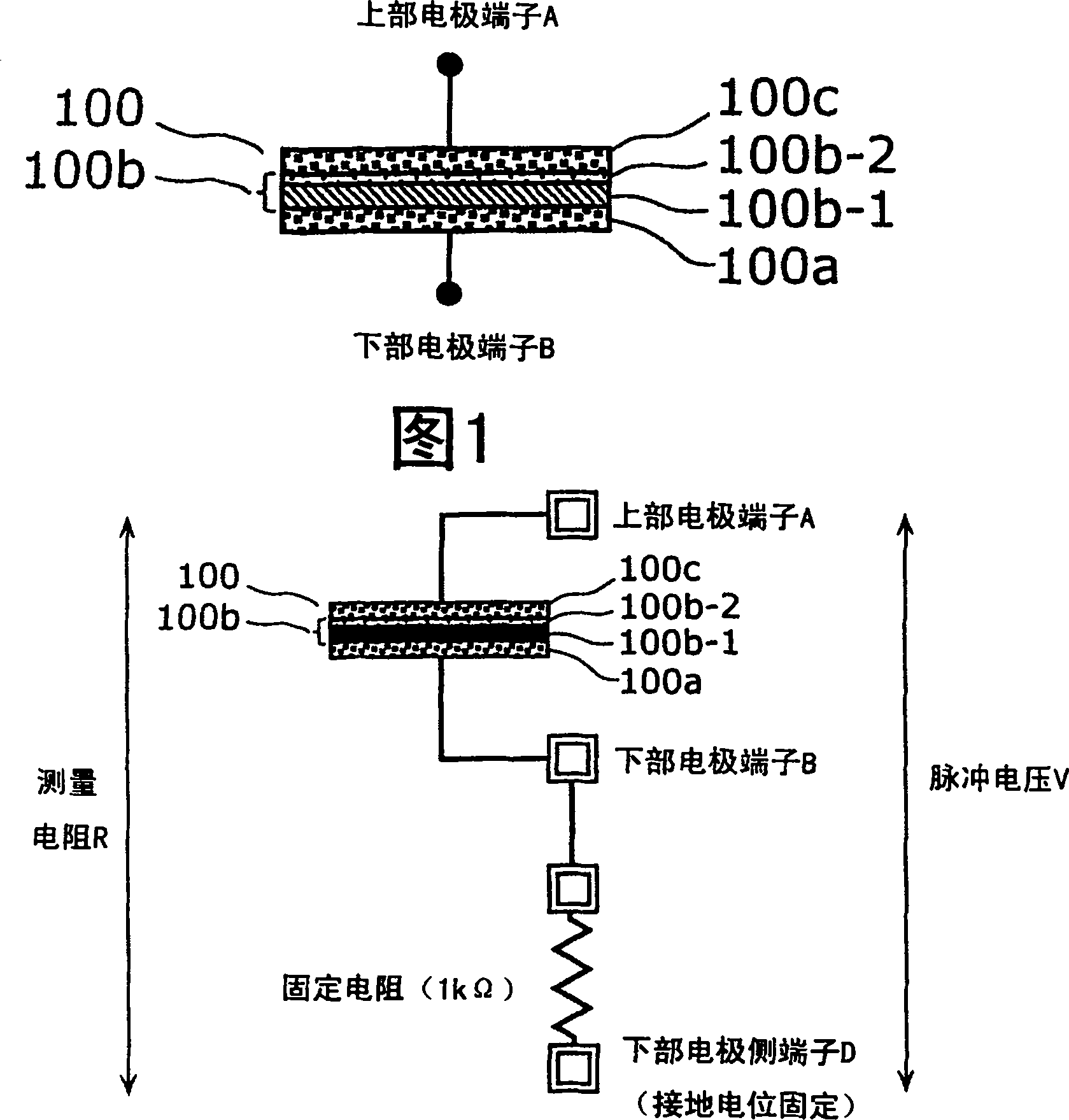
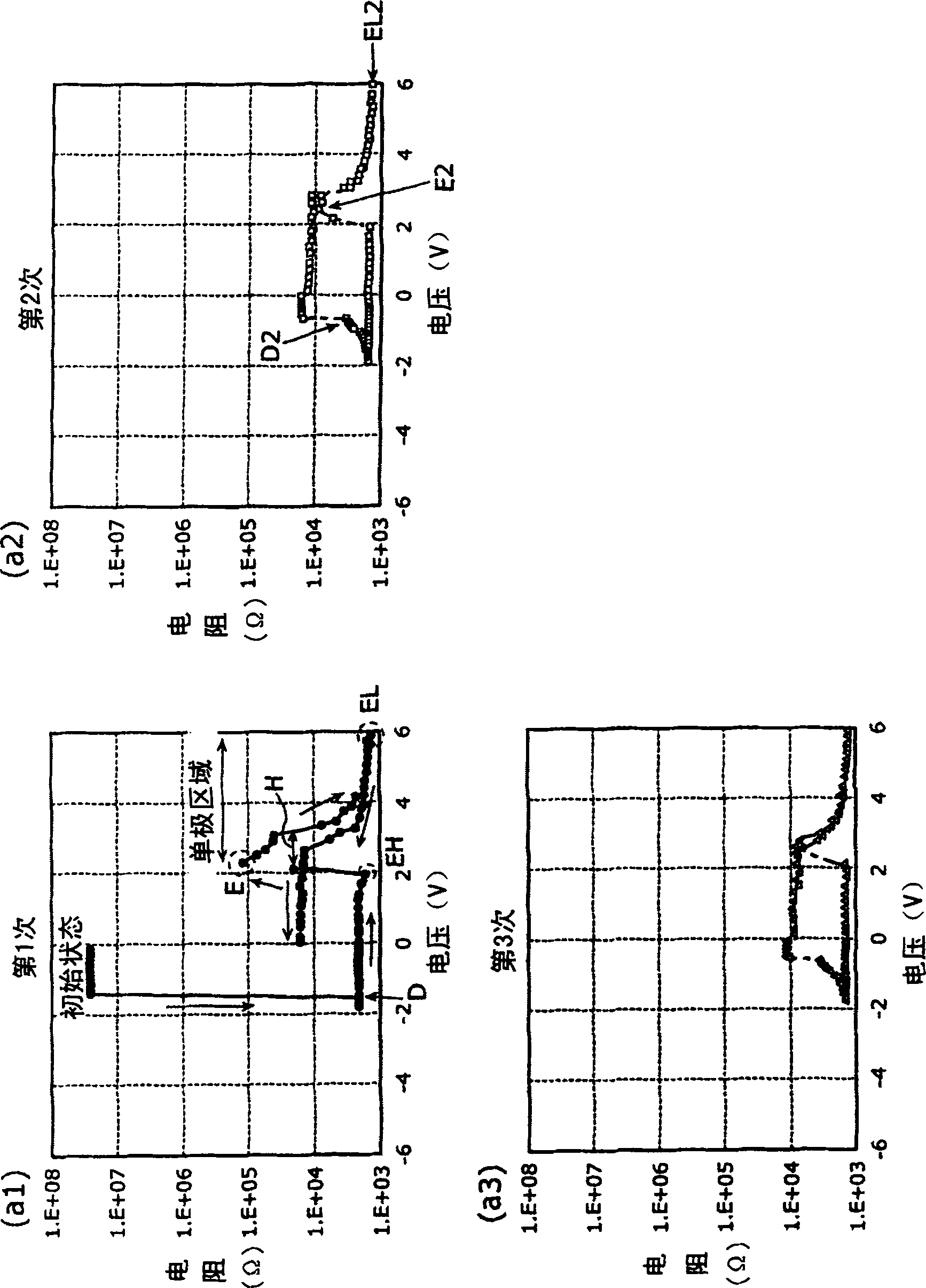
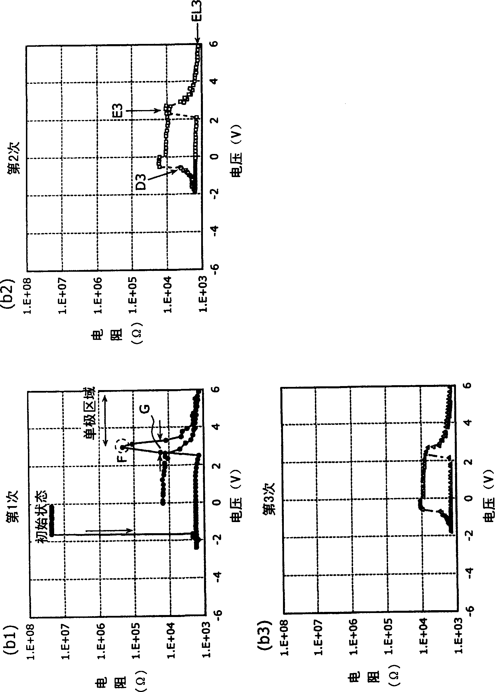
[0127] The variable resistance nonvolatile memory device in the first embodiment of the present invention is a 1T1R nonvolatile memory device in which a variable resistance element and a MOS transistor are connected in series, and is used to provide a variable resistance element capable of controlling The high resistance level molding method and the most suitable high resistance pulse voltage application to the variable resistance element, so the high resistance state and the low resistance state have a wide operating window.

[0128] [Basic data of the present invention 1 Characteristics of variable resistance films with fixed resistance elements connected in series]

[0129] As preparation for the description, basic data related to the variable resistance element used in the variable resistance nonvolatile memory device of the present invention will be described.

[0130] figure 1 It is a schematic diagram showing the basic structure of the variable resistance element used in this...


PUM


Abstract

An optimum forming method of performing a forming for a variable resistance element to maximize an operation window of the variable resistance element is provided. The forming method is used to initialize a variable resistance element (100). The forming method includes: a determination step (S35) of determining whether or not a current resistance value of the variable resistance element (100) is lower than a resistance value in a high resistance state; and a voltage application step (S36) of applying a voltage pulse having a voltage not exceeding a sum of a forming voltage and a forming margin when the determination is made that the current resistance value is not lower than the resistance value in the high resistance state (No at S35). The determination step (S35) and the voltage application step (S36) are repeated to process all memory cells in a memory array (202) (S34 to S37).

Description

Technical field [0001] The present invention relates to a forming (initialization) method for stably changing the resistance of a variable resistance nonvolatile memory element whose resistance value changes reversibly in accordance with an electrical signal, and a variable resistance nonvolatile memory having that function Device. Background technique [0002] In recent years, a resistance variable nonvolatile memory device (hereinafter also simply referred to as a variable resistance nonvolatile memory device) having a memory cell composed of a variable resistance nonvolatile memory element (hereinafter also simply referred to as a "Non-volatile storage devices".) Research and development. The so-called variable resistance element refers to an element that has a property that the resistance value changes reversibly in accordance with an electrical signal, and can further store data corresponding to the resistance value in a nonvolatile manner. [0003] As a non-volatile memory ...

Claims


Application Information

Patent Timeline
Patent Type & Authority Patents(China)
IPC IPC(8): G11C13/00
CPCG11C2213/32G11C2213/34H01L45/146G11C13/0069G11C13/0007G11C2013/0083G11C2213/79H01L27/101H01L27/2436H01L45/08G11C13/0064H10B63/30H10N70/24H10N70/8833H10N70/826
Inventor 河合贤岛川一彦村冈俊作东亮太郎
Owner PANASONIC SEMICON SOLUTIONS CO LTD
Why Eureka
Try Eureka