

Light-emitting apparatus
A light-emitting device and light-emitting device technology, applied in the direction of lighting devices, electroluminescent light sources, light sources, etc., can solve the problems of completely preventing shadowing, reducing the accuracy of the second electrode, and manufacturing steps and difficulties without success
- Summary
- Abstract
- Description
- Claims
- Application Information
AI Technical Summary
Problems solved by technology
Method used
Image

Examples
no. 1 example
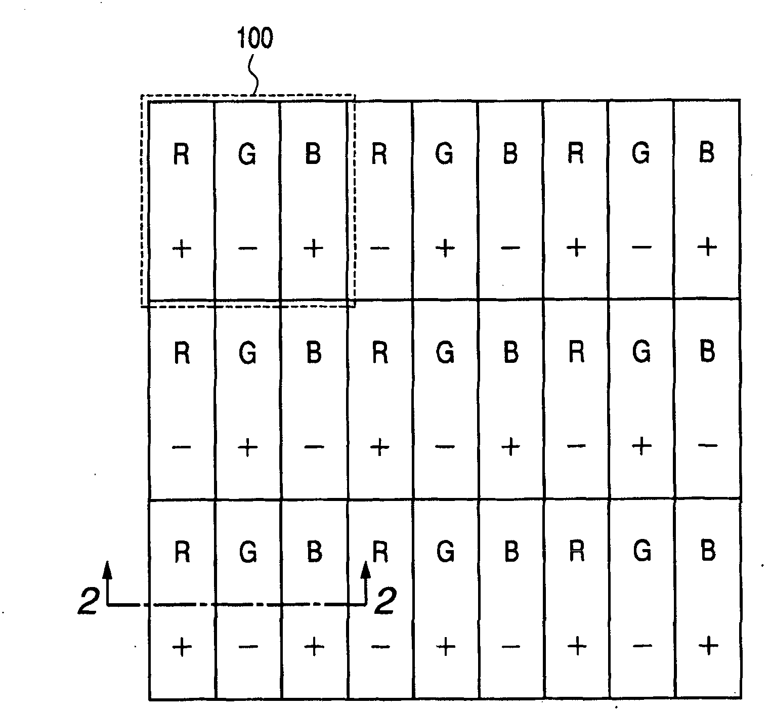
[0031] figure 1 An example is shown in which the light emitting device according to the first embodiment of the present invention is used as a display. The pixel 100 is composed of three sub-pixels R, G, and B, which respectively include organic EL light-emitting devices of three different colors, that is, red (R), green (G) and blue (B). .
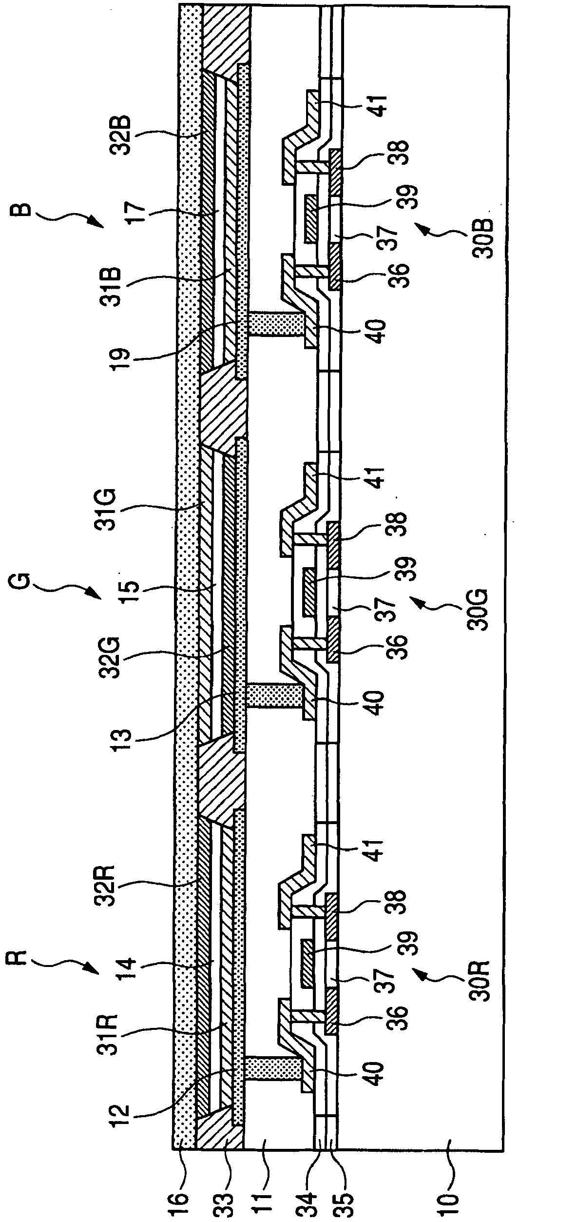
[0032] figure 2 is along figure 1 A cross-sectional view of a single pixel 100 taken at line 2-2.
[0033] The R subpixel is driven by a thin film transistor (TFT) 30R. The R subpixel includes, on the lower electrode 12 connected to the drain electrode 40 of the TFT 30R, a hole injection layer 31R, a light emitting layer 14 , and an electron injection layer 32R stacked in this order and covered by the upper electrode 16 .
[0034] The G subpixel following the R subpixel is driven by a thin film transistor (TFT) 30G. The G sub-pixel includes, on the lower electrode 13 connected to the drain electrode 40 of the TFT 30G, an electron i...
no. 2 example
[0053] Figure 4 The pixel arrangement of is a modification of the first embodiment, in which the three sub-pixels R, G, and B of the pixel 100 have a layer structure that directs a direction of a certain direction current of one sub-pixel ((+ ) connection or (-) connection) is set to be opposite to the direction of the current in a certain direction of its adjacent sub-pixel, and the direction of the current in a certain direction of a sub-pixel of one color in the pixel ((+) connection or ( -) connected) is the same as the direction of the certain direction current of the sub-pixel of the same color in its adjacent pixel. exist Figure 4 In , only the G light emitting device is connected in the (-) direction, and the R and B light emitting devices are connected in the (+) direction.
[0054] This embodiment changes the direction in which the organic EL device is electrically connected to the common electrode (Vc) for different colors. An organic EL device whose colors R, ...
no. 3 example
[0057] exist Figure 5A and Figure 5B A sub-pixel arrangement according to a third embodiment of the present invention is shown in .
[0058] In the present embodiment, the pixel 100 is formed of two sub-pixels 100a and 100b that emit light of two different colors at different time points. Figure 5A and Figure 5B The colors of light emitted by subpixels 100a and 100b in two different subfields are shown. These two subfields are actually combined into one frame of the image.
[0059] The sub-pixel 100a alternately emits red (R) light and blue (B) light. The sub-pixel 100b alternately emits green (G) light and blue (B) light. The sub-pixels 100a and 100b are arranged in a fixed pattern, and the pattern is cyclically repeated in the row direction and the column direction.
[0060] exist Figure 5A and Figure 5B In the example of , the sub-pixel 100a and the sub-pixel 100b of a single pixel emit blue light in turn. Pixels 100a and 100b do not emit red and green light ...
PUM
 Abstract
Description
Claims
Application Information