Method for cleaning polymer on side wall of etching chamber and contact hole forming method

A technology for etching cavity and polymer, applied in cleaning methods and appliances, chemical instruments and methods, electrical components, etc., can solve problems such as small contact hole line width and failure to reach the target size

Inactive Publication Date: 2011-06-15
SEMICON MFG INT (SHANGHAI) CORP +1
View PDF1 Cites 7 Cited by
  • Summary
  • Abstract
  • Description
  • Claims
  • Application Information

AI Technical Summary

Problems solved by technology

[0006] However, after the above cleaning method cleans the etching chamber, because the polymer is cleaned too cleanly, the line width after the subsequent contact hole etching is too small, and the target size cannot be reached.

Method used


Image

  • Method for cleaning polymer on side wall of etching chamber and contact hole forming method
  • Method for cleaning polymer on side wall of etching chamber and contact hole forming method
  • Method for cleaning polymer on side wall of etching chamber and contact hole forming method

Examples


Embodiment Construction

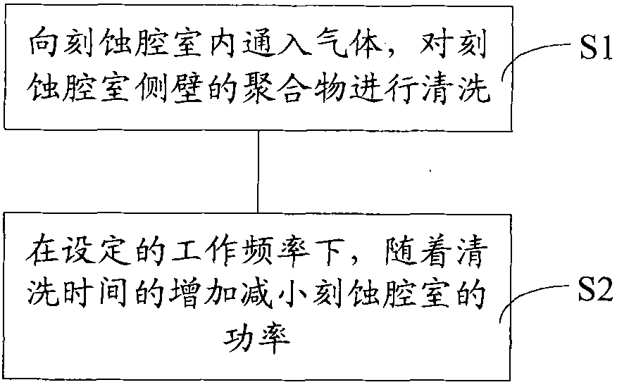
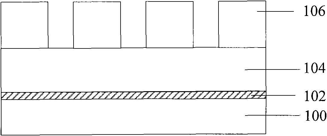
[0024] In the prior art, in the process of etching the insulating dielectric layer to form a contact hole, because too much polymer remains on the side wall of the etching chamber, when the contact hole is formed by subsequent etching, the polymerization formed on the side wall of the etching chamber will Excessive accumulation of particles will cause excessive particles on the surface of the wafer, resulting in incomplete etching of contact holes or short circuits. However, if the polymer on the side wall of the etching chamber is cleaned and there is too little residue, the line width after subsequent contact hole etching will be too small and the target size will not be reached.

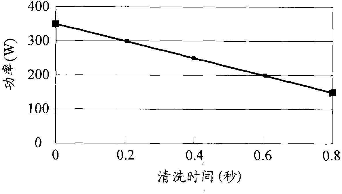
[0025] In order to solve the above problems, the present invention adopts a new method for cleaning the sidewall polymer of the etching chamber, and the specific process is as follows figure 1 As shown, step S1 is performed to inject gas into the etching chamber to clean the polymer on the side wa...


PUM


Abstract

The invention discloses a method for cleaning a polymer on the side wall of an etching chamber and a contact hole forming method. The method for cleaning the polymer on the side wall of the etching chamber comprises: introducing a gas into the etching chamber, and setting a preset working frequency; and reducing the power of the etching chamber whole the cleaning time increases, and obtaining theoptimal thickness of the polymer on the side wall of the etching chamber. In the invention, the line width of a contact hole formed in the etching chamber reaches a target size.

Description

technical field [0001] The invention relates to the technical field of semiconductor manufacturing, in particular to a method for cleaning the sidewall polymer of an etching chamber and a method for forming a contact hole. Background technique [0002] In the manufacture of integrated circuits, materials deposited on semiconductor substrates, such as silicon dioxide, silicon nitride, polysilicon, metal, metal silicide, and single crystal silicon, are usually etched in a predetermined pattern by an etching process. gates, vias, contact holes, trenches or interconnect lines. [0003] During the etching process, etch residues (often referred to as polymers) are deposited on the walls of the etch chamber and on the surfaces of other components. The composition of the etch residue depends on the type of evaporated etching gas, the The material to be etched, and the chemical composition of the mask layer on the substrate. For example, when a metal layer, such as aluminum, etc. i...

Claims


Application Information

Patent Timeline
Patent Type & Authority Applications(China)
IPC IPC(8): B08B7/00H01L21/768
Inventor 张海洋尹晓明孙武黄怡
Owner SEMICON MFG INT (SHANGHAI) CORP
Why Eureka
Try Eureka