

Cleaning machine table for semiconductor package products and cleaning process thereof
A technology for semiconductors and washing machines, which is applied in the direction of cleaning methods using liquids, semiconductor/solid-state device manufacturing, cleaning methods and appliances, etc., which can solve the problem of equipment or processes without residual glue, residual glue performance and functional testing. Large impact and other issues, to achieve the effect of convenient product function test, good cleaning effect and fast cleaning speed
- Summary
- Abstract
- Description
- Claims
- Application Information
AI Technical Summary
Problems solved by technology
Method used
Image

Examples
Embodiment Construction
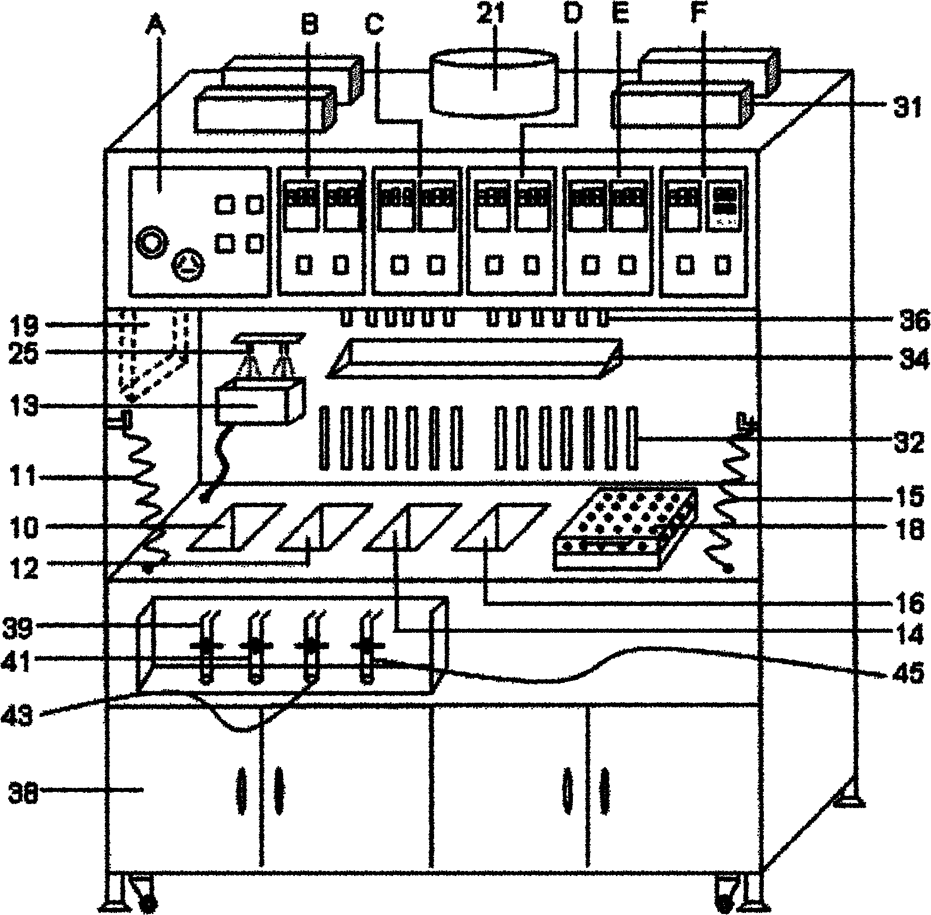
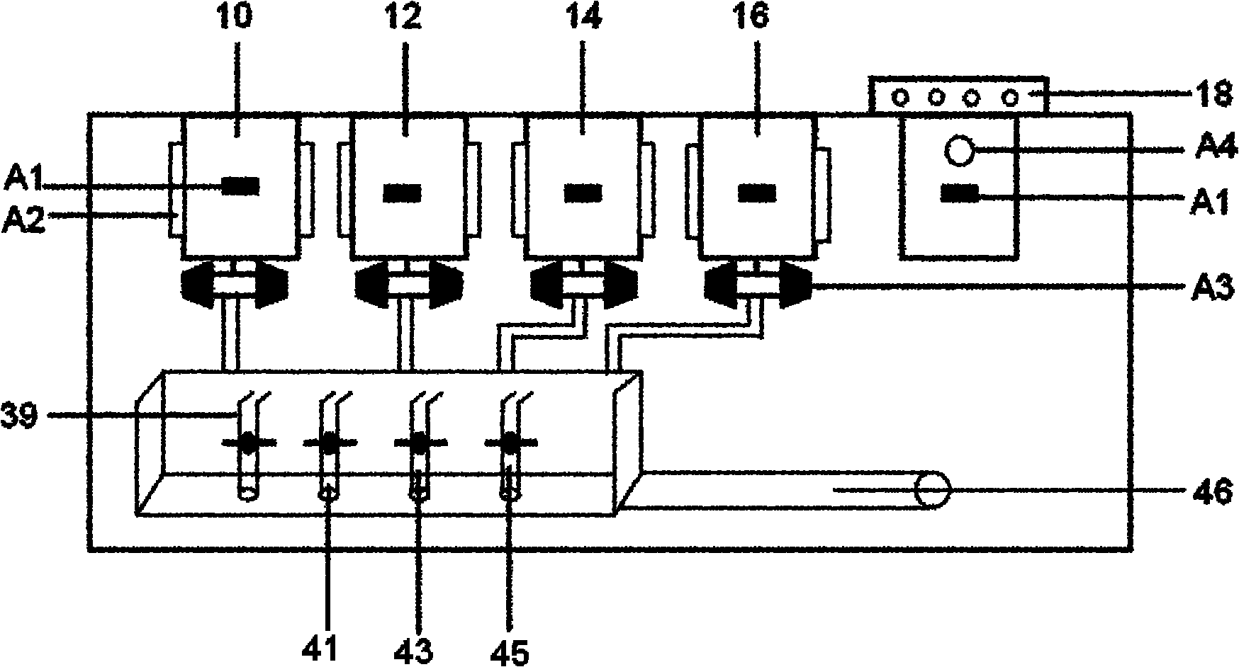
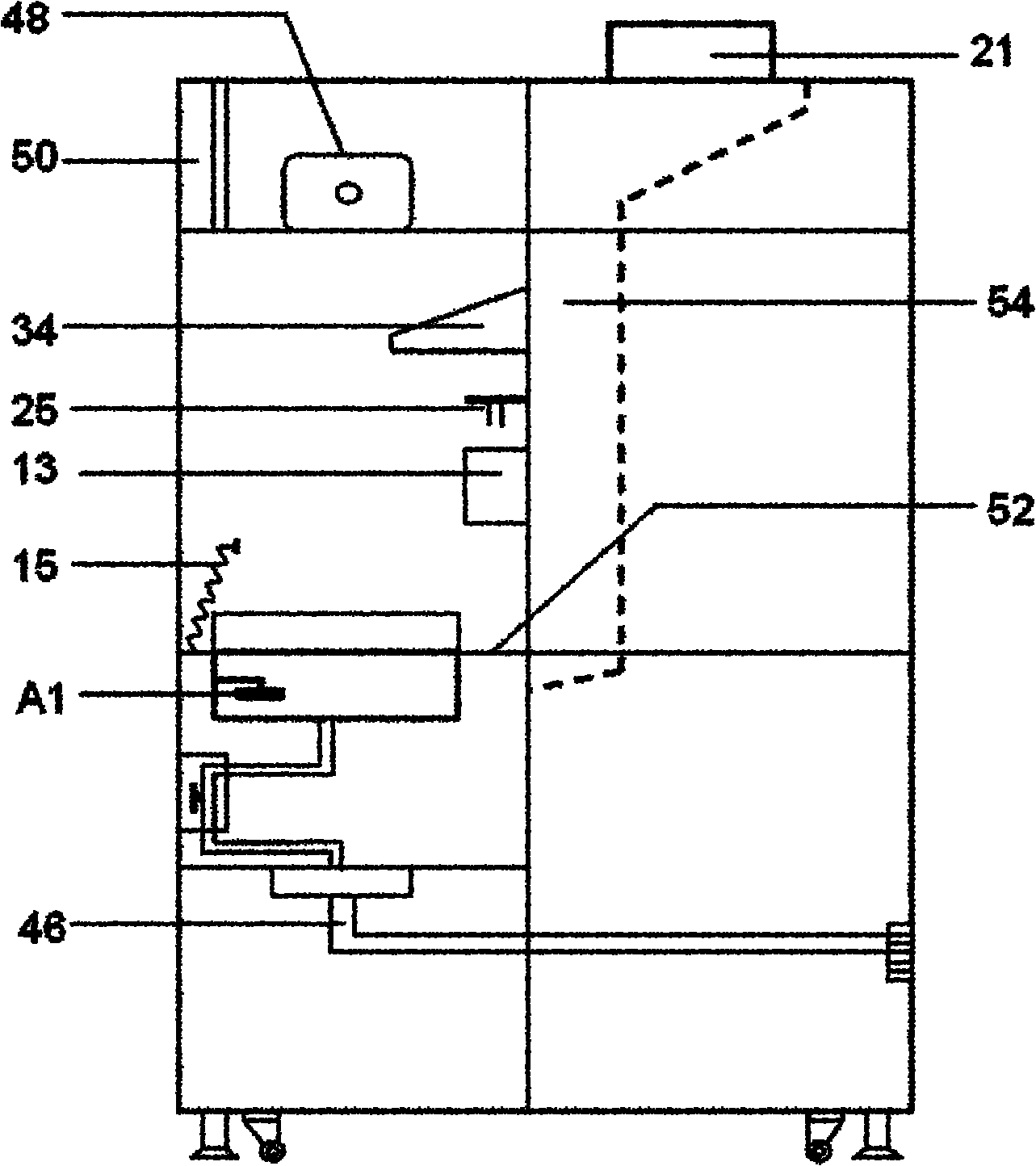
[0032] The present invention proposes a chip cleaning machine used in the semiconductor packaging process and a cleaning process, wherein the cleaning machine includes a control panel, a cleaning operation area and a drying area, and the control panel is located on the upper part of the front of the machine for realizing Control of the cleaning process; the cleaning operation area is located in the middle of the front of the machine and is in the shape of a hollow tank. The operation area includes more than one cleaning tank, and the cleaning machine is equipped with an ultrasonic generator corresponding to each cleaning tank to use ultrasonic waves to clean each cleaning tank. The encapsulated semiconductor chips in the groove are cleaned; and the drying area is used for drying the cleaned chips.
[0033] Preferably, a table top is provided in the cleaning operation area, and the above-mentioned cleaning tank includes more than one chemical tank and more than one water tank. T...
PUM
 Abstract
Description
Claims
Application Information