Method for manufacturing cmos image sensor

A technology of image sensor and manufacturing method, applied in semiconductor/solid-state device manufacturing, semiconductor device, electric solid-state device, etc., can solve the problems of reduced device yield and defective devices, reduce thermal budget, prevent interconnection delamination, etc. , Improve the effect of dark characteristics

Inactive Publication Date: 2011-06-15
INTELLECTUAL VENTURES II
View PDF6 Cites 4 Cited by
  • Summary
  • Abstract
  • Description
  • Claims
  • Application Information

AI Technical Summary

Problems solved by technology

However, if figure 1 As shown, interconnect delamination occurs due to high temperature heat treatment, so that the yield of the device decreases and the device may become defective

Method used


Image

  • Method for manufacturing cmos image sensor
  • Method for manufacturing cmos image sensor
  • Method for manufacturing cmos image sensor

Examples


Embodiment

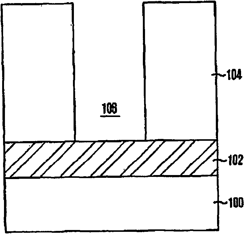
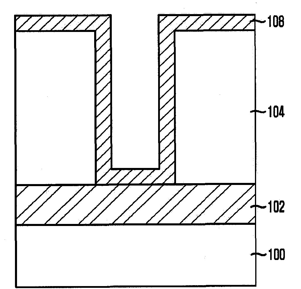
[0026] Figures 2 to 8 is a cross-sectional view illustrating a method of manufacturing a CMOS image sensor according to an embodiment of the present invention.

[0027] Such as figure 2 As shown, a first metal interconnection 102 is formed on a substrate 100 including a semiconductor structure including a plurality of transistors and a photodiode serving as a light receiving device. In this case, the first metal interconnection 102 may include one selected from the group consisting of aluminum (AL), copper (Cu), tungsten (W), or platinum (Pt). Preferably, the first metal interconnection 102 includes Al.

[0028] Then, an insulating interlayer 104 is formed on the substrate 100 to cover the first metal interconnection 102 . In this case, the interlayer insulating layer 104 includes oxide, preferably, silicon oxide (SiO 2 ). For example, the interlayer insulating layer 104 may include a material made of BPSG (borophosphosilicate glass) film, PSG (phosphosilicate glass) fi...


PUM


Abstract

An object of the present invention is to provide a method for manufacturing a CMOS image sensor, capable of preventing hillock defects caused by a wire lifting phenomenon in a CMOS image sensor. To this end, the present invention provides a method for manufacturing a CMOS image sensor, including the steps of: preparing a substrate on which a first metal wire is formed; forming an interlayer insulating layer on the first metal wire; etching the interlayer insulating layer to form a contact hole for exposing a part of the first metal wire; forming a buffer layer on the interlayer insulating layer along an inner surface of the contact hole; performing a heat treatment process; etching the buffer layer to form a spacer on an inner wall of the contact hole; forming a barrier metal layer along an upper surface of the interlayer insulating layer including the spacer; forming a contact plug on the barrier metal layer such that the contact hole is buried; and forming a second metal wire on theinterlayer insulating layer such that the second metal wire is connected to the contact plug.

Description

technical field [0001] The present invention relates to semiconductor manufacturing technology, and more particularly, to a method of forming a contact plug for manufacturing a CMOS image sensor including metal interconnections having a multilayer structure. Background technique [0002] In a manufacturing method of a CMOS image sensor, in order to improve dark characteristics, a high temperature heat treatment is performed after depositing a passivation layer. However, if figure 1 As shown, interconnection delamination may occur due to high temperature heat treatment, so that the yield of the device decreases and the device may become defective. This is due to heat treatment at high temperature for a long time after the passivation layer has been formed. Contents of the invention [0003] technical problem [0004] The present invention has been made to solve the problems arising in the prior art, and an object of the present invention is to provide a method of manufac...

Claims


Application Information

Patent Timeline
Patent Type & Authority Applications(China)
IPC IPC(8): H01L27/146
CPCH01L21/76826H01L21/76831H01L27/14689H01L27/14687H01L27/146
Inventor 表成奎
Owner INTELLECTUAL VENTURES II
Why Eureka
Try Eureka