Film adhering method and device of wafer

A film sticking device and wafer technology, applied in electrical components, semiconductor/solid-state device manufacturing, circuits, etc., can solve the problems of reducing chip yield, affecting wafer quality, not non-contact film sticking, etc., to reduce damage to crystals. The risk of rounding the front, reducing the risk of re-filming, the effect of high filming efficiency

Inactive Publication Date: 2013-01-23
上海技美科技股份有限公司
View PDF6 Cites 0 Cited by
  • Summary
  • Abstract
  • Description
  • Claims
  • Application Information

AI Technical Summary

Problems solved by technology

[0008] 3. Wafers of different thicknesses can withstand different pressures
[0009] 4. The film attaching device in the prior art can only be applied to wafers of one size. When attaching films to wafers of different sizes, it is necessary to replace the table of the corresponding size, which increases the operation steps and reduces the production efficiency.
[0010] In addition, the method described above is not a non-contact film in the true sense
The wafer is in contact with the supporting device, even if the contact area is small, it will still affect the quality of the wafer and reduce the yield of the chip

Method used


Image

  • Film adhering method and device of wafer
  • Film adhering method and device of wafer
  • Film adhering method and device of wafer

Examples


Embodiment 1

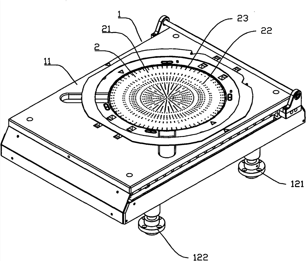
[0050] Such as figure 1 As shown, the wafer attaching device includes a base 1. Four seat legs (two seat legs 121 and 122 are shown in the figure) are installed on the lower surface of the base 1 to support the base 1. The upper surface 11 of the base 1 is provided with a first groove (not shown in the figure) for receiving the first plate 2.

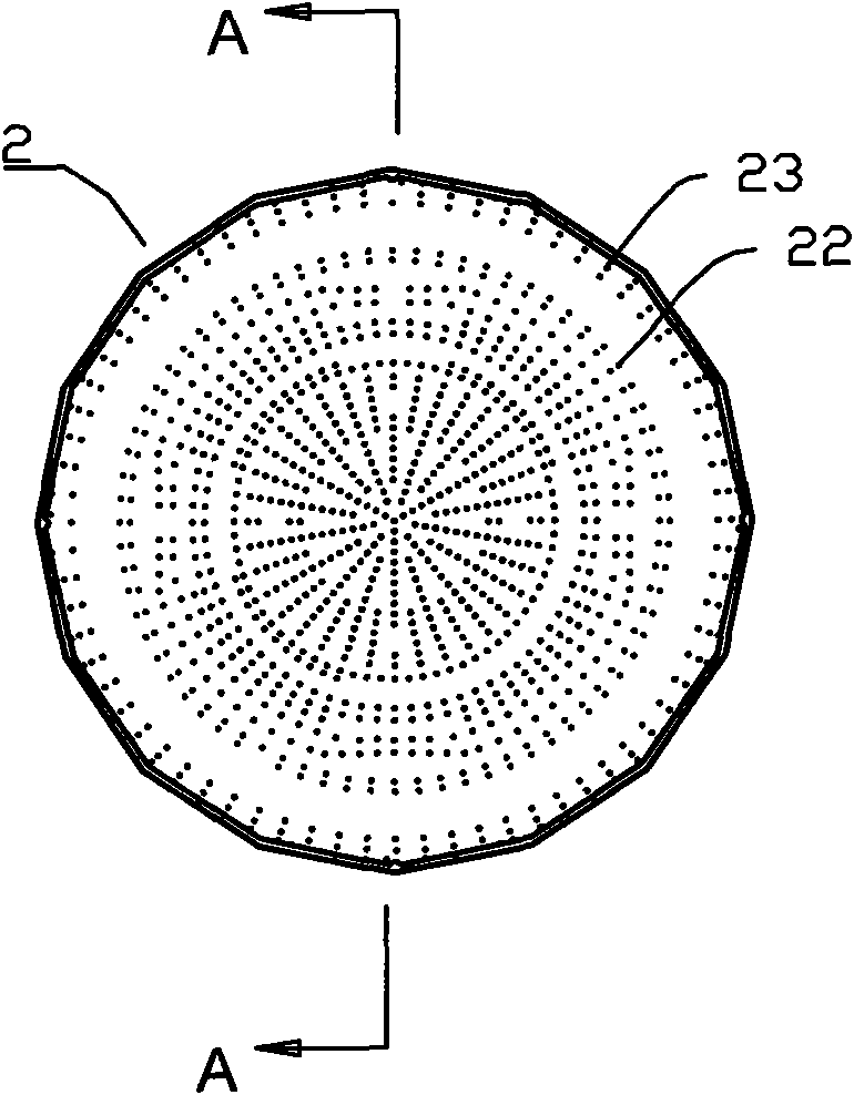
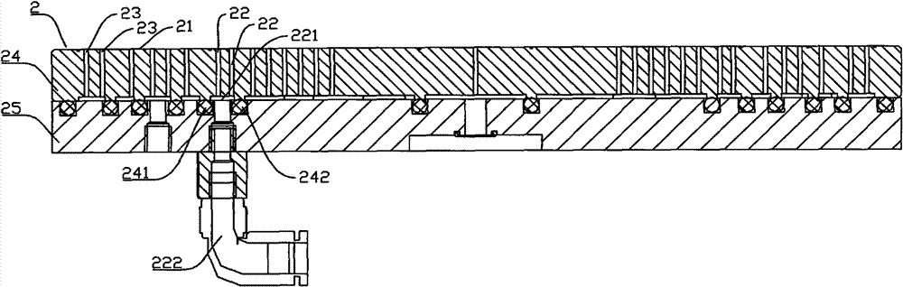
[0051] Such as figure 1 As shown, the first plate 2 is circular. The upper surface 21 of the first plate 2 is provided with a plurality of first air holes 22, the number of which can be determined according to the diameter of the first plate 2. The number of first air holes 22 in each circle is more than two, which are evenly distributed along the circumferential direction, and the specific number can be determined according to the circumferential length. The first air hole 22 extends from the upper surface of the first platen 2 to the lower surface. The first air holes 22 are in communication with an air compressor (not shown in the fi...

Embodiment 2

[0055] Figure 4 It is a schematic structural diagram of Embodiment 2 of the present invention. Such as Figure 4 As shown, the wafer sticking device includes a base 1, and four seat legs are installed on the lower surface of the base 1 to support the base 1. Figure 4 Only two legs (121, 122) are shown in.

[0056] The upper surface 11 of the base 1 is provided with a first groove (not shown in the figure). The first groove is used to accommodate the first disc 2. The structure and usage of the first tray 2 are the same as those in the first embodiment. The size of the first tray 2 is equivalent to that of a 12-inch wafer. The edge of the 12-inch wafer can be sucked and fixed on the first tray 2 through the second air hole 23. The compressed air can be blown between the 12-inch wafer and the first tray 2 through the first air hole 22 to provide support for the 12-inch wafer.

[0057] The upper surface 21 of the first plate 2 is provided with a second groove (not shown in the f...

Embodiment 3

[0069] The difference between this embodiment and the second embodiment is that the first plate 2 and the cylinder are not provided. The second platen 3 is arranged in the first groove of the base 1, and the size of the first groove is adapted to the diameter of the second platen 3. The rest of the structure is the same as the second embodiment.

[0070] This embodiment is only applicable to wafers with one size of film, but either non-contact film or contact film can be used.


PUM


Abstract

The invention discloses a film adhering method of a wafer. The film adhering method of the wafer is characterized by comprising the following steps of: blowing a gas between the wafer and a table disc; supporting the wafer by utilizing the blown gas; and then adhering a film on the surface of the wafer. By using the film adhering method and device of the wafer, the non-contact film adhesion can be realized and the danger of front surface damage of the wafer can be reduced; in addition, because the wafer can be supported by utilizing the gas during the pressing of a roller wheel, the pressure of the roller wheel can be offset, and the roller wheel can not be easy to press the wafer to be broken or crushed, therefore when the film adhering method and device are used for carrying out the non-contact film adhesion, the minimum thickness of the wafer which can be adhered with the film is 50 micrometers and 200 micrometers far less than that of the water adhered with the film in the prior art.

Description

technical field [0001] The invention relates to a method for attaching a film to a wafer and a device for attaching a film to a wafer. Background technique [0002] Usually, the circuit side of the wafer, that is, the side that completes the chip function, is called the front side, and the other side is the back side. During wafer processing, for various purposes, it is often necessary to stick a thin film on the surface of the wafer. There is a kind of film to protect the wafer when cutting the wafer, which is called dicing film, and the dicing film is attached to the back of the wafer. Some films play a protective role in other processes. A frame is required for wafer dicing, and the frame is a sheet with a through hole in the middle. The wafer is located in the through hole of the frame, and both are pasted on the same film. When attaching a dicing film to a wafer, it is necessary to attach the wafer and the frame to the dicing film together. The frame and the dicing...

Claims


Application Information

Patent Timeline
Patent Type & Authority Patents(China)
IPC IPC(8): H01L21/02H01L21/00
Inventor 张明星
Owner 上海技美科技股份有限公司
Why Eureka
Try Eureka