Method and system for detecting material defects based on photonuclear reaction
A technology for detecting materials and defects, applied in the direction of material analysis using measurement of secondary emissions, and can solve problems such as inability to detect
- Summary
- Abstract
- Description
- Claims
- Application Information
AI Technical Summary
Problems solved by technology
Method used
Image
Examples
Embodiment Construction
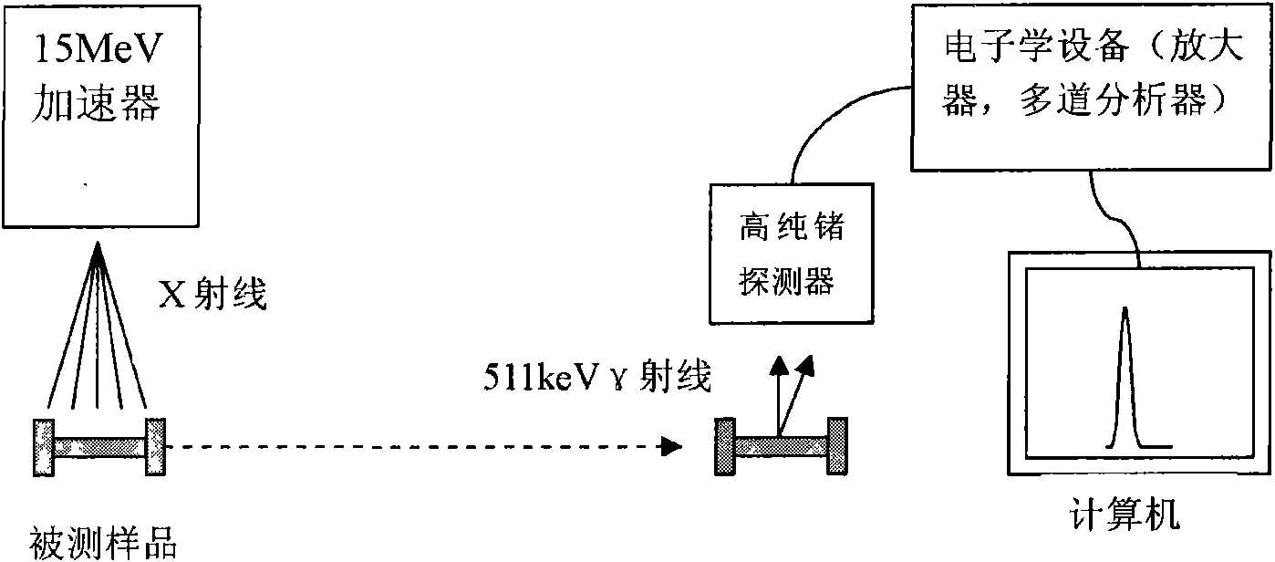
[0016] figure 1 It is a schematic diagram of the system for detecting material defects based on photonuclear reaction of the present invention. As shown in the figure, the high-energy X-rays generated by the 15MeV electron accelerator scan the sample under test. Because X-rays have strong penetrating power in the material, they can penetrate deep into the sample, instead of ordinary positrons, which can only analyze the surface layer. After X-ray penetrates into the material, it can interact with some parts of the sample. A photoneutron reaction occurs in the nucleus, causing the nucleus to lose a neutron. After the neutron is lost, the nucleus becomes a neutron-deficient nucleus, so it has β+ radioactivity and can emit positrons, so that positrons are generated inside the sample.
[0017] In the photopositron analysis technology of the present invention, the radiation source used is X-rays generated by a high-energy electron accelerator. The energy of the accelerator is require...
PUM
 Abstract
Description
Claims
Application Information


