Semiconductor element and method for forming the same

A semiconductor and component technology, applied in the field of high-voltage semiconductor components and their formation, can solve the problems of increasing IC manufacturing process and production complexity, and achieve the effect of high blocking voltage

Active Publication Date: 2011-06-29
TAIWAN SEMICON MFG CO LTD
View PDF8 Cites 5 Cited by
  • Summary
  • Abstract
  • Description
  • Claims
  • Application Information

AI Technical Summary

Problems solved by technology

The above-mentioned progress will increase the complexity of IC manufacturing process and production. In order to make the progress easy to understand, the development of IC manufacturing process requires similar production methods and development.

Method used


Image

  • Semiconductor element and method for forming the same
  • Semiconductor element and method for forming the same
  • Semiconductor element and method for forming the same

Examples


Embodiment Construction

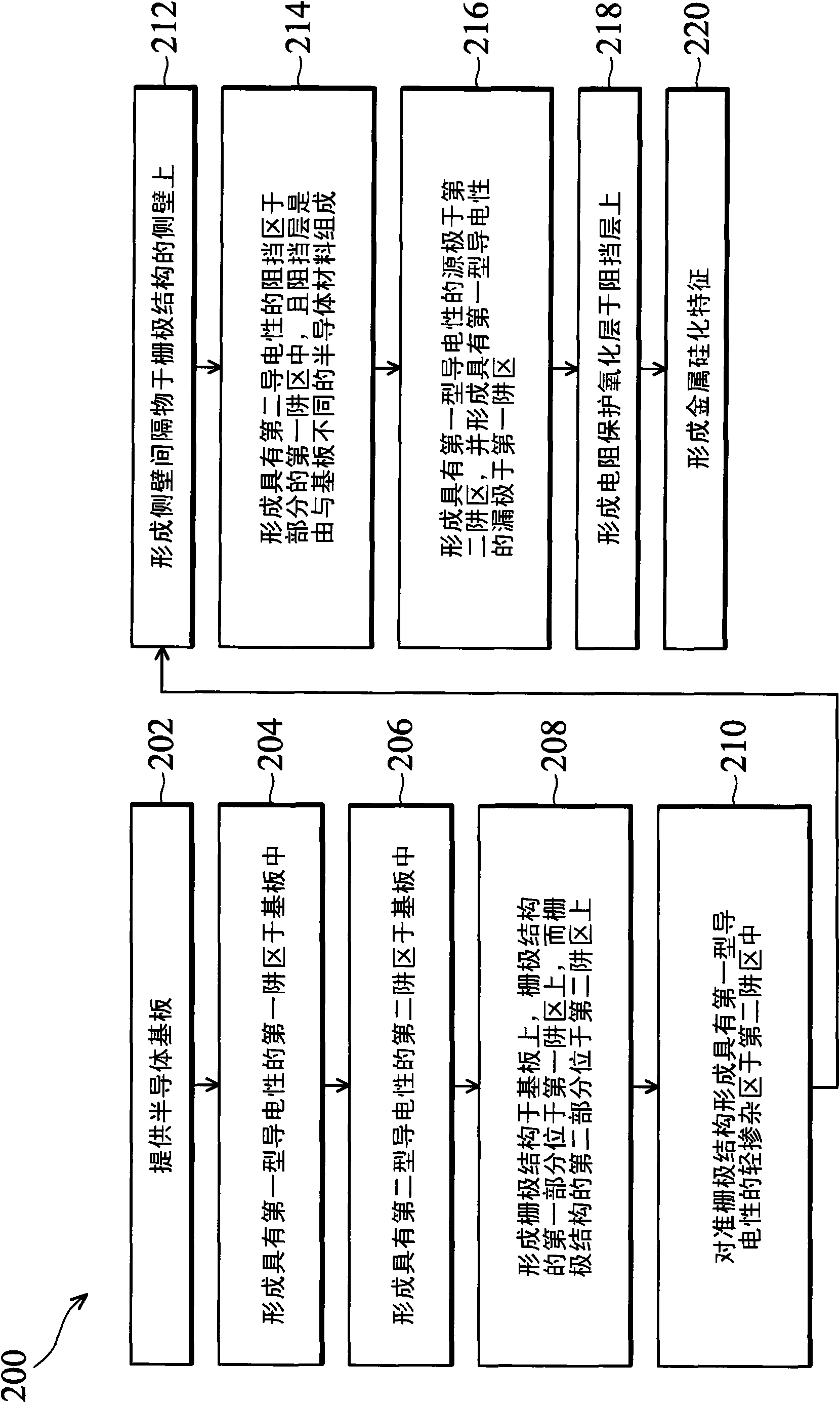
[0013] The field of the invention is semiconductor integrated circuits. It is to be understood that the following disclosure provides various examples to illustrate various features of the invention. In order to simplify the description, specific embodiments, units, and combinations will be used for description. However, these specific examples are not intended to limit the present invention. In addition, in order to simplify the description, the present invention uses the same symbols in different drawings to indicate similar components in different embodiments, but the above repeated symbols do not mean that the components in different embodiments have the same corresponding relationship. On the other hand, forming an element on another element includes the two elements being in direct contact, or the two elements being separated by other elements.

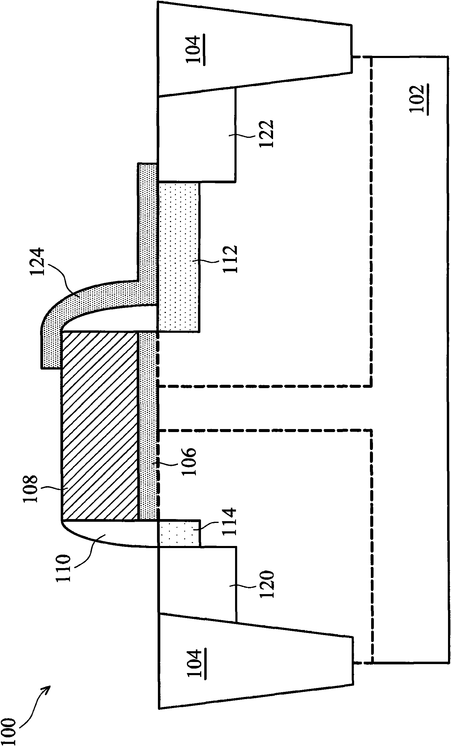
[0014] figure 1 It is a cross-sectional view of a high-voltage semiconductor device 100, which is formed by a CMOS manufact...


PUM


Abstract

The invention provides a semiconductor element and a method for forming the same. The semiconductor device includes a semiconductor substrate, a gate structure formed on the substrate, sidewall spacers formed on each side of the gate structure, a source and a drain formed in the substrate on either side of the gate structure, the source and drain having a first type of conductivity, a lightly doped region formed in the substrate and aligned with a side of the gate structure, the lightly doped region having the first type of conductivity, and a barrier region formed in the substrate and adjacent the drain. The barrier region is formed by doping a dopant of a second type of conductivity different from the first type of conductivity. The semiconductor element formed in the invention possesses high blocking voltage.

Description

technical field [0001] The invention relates to a semiconductor technology, in particular to a high-voltage semiconductor element and its forming method. Background technique [0002] The semiconductor integrated circuit industry has grown rapidly for some time. Advances in the materials and design of integrated circuits have made each generation of integrated circuits smaller and more complex than the previous generation. The above-mentioned advances will increase the complexity of the IC manufacturing process and production. In order to make the progress easy to understand, the development of the IC manufacturing process requires similar production methods and developments. [0003] When complementary metal-oxide-semiconductor field-effect transistors (CMOSFETs) are used in the high-voltage field, it is necessary to integrate high-voltage devices and low-voltage devices (such as logic devices or storage devices) to be applied on a system-on-chip (SoC). For example, a lat...

Claims


Application Information

Patent Timeline
Patent Type & Authority Applications(China)
IPC IPC(8): H01L29/78H01L29/06H01L21/336
CPCH01L29/0646H01L29/66659H01L29/165H01L29/456H01L29/7835H01L29/4933H01L29/665H01L29/0847
Inventor 张立伟朱鸣庄学理
Owner TAIWAN SEMICON MFG CO LTD
Why Eureka
Try Eureka