Semiconductor Device and a Method of Manufacturing Same

Inactive Publication Date: 2016-04-14
HITACHI LTD +1
View PDF4 Cites 6 Cited by
  • Summary
  • Abstract
  • Description
  • Claims
  • Application Information

AI Technical Summary

Benefits of technology

[0018]With the semiconductor device according to the present invention, since the passivation film includes the first through the third silicon oxide films, an electric field applied on the passivation film is relaxed, and the passivation film can be provided without the need for a particular process and material, so that productio

Problems solved by technology

However, the SiC semiconductor device has the problem of an increase in leakage current, and breakage of a passivation film because of high electric fields applied on the passivation film.
Further, upon an increase in the number of the traps, large current flows, thereby leading to the breakage of the passivation film.
With the termination

Method used


Image

  • Semiconductor Device and a Method of Manufacturing Same
  • Semiconductor Device and a Method of Manufacturing Same
  • Semiconductor Device and a Method of Manufacturing Same

Examples


first embodiment

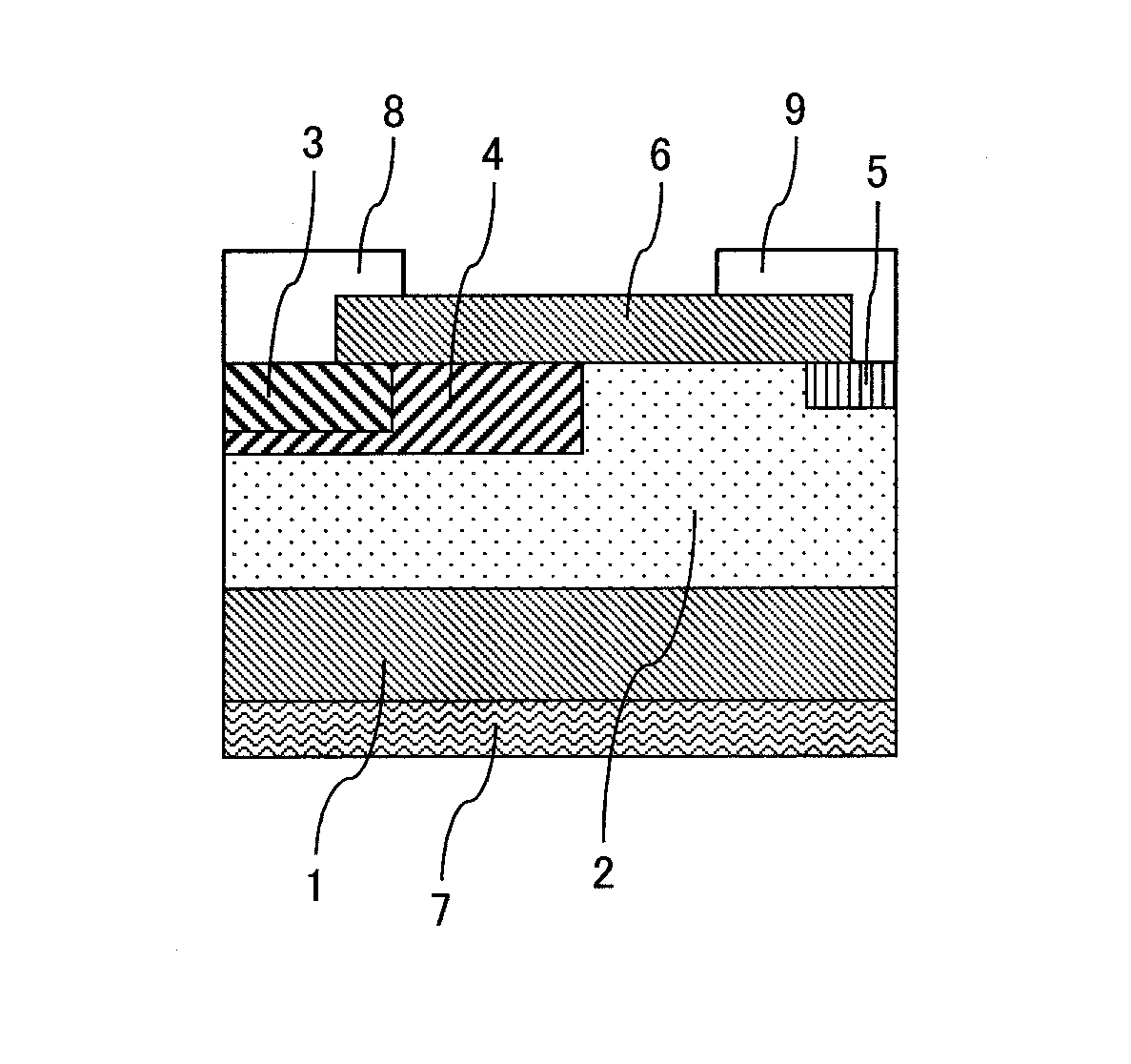
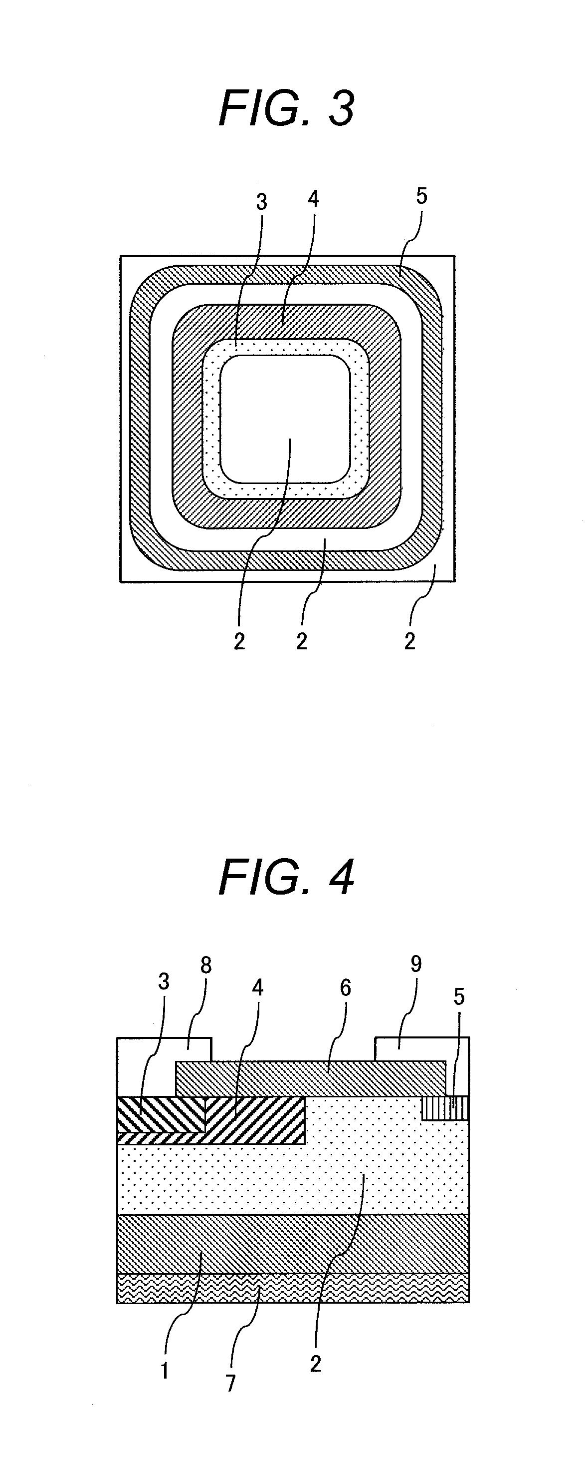
[0026]FIG. 1 is a longitudinal sectional view showing a termination region of an SiC semiconductor device according to one embodiment of the present invention. A termination structure according to the present embodiment is applicable to a power device such as a high blocking voltage diode, and a high blocking voltage MOSFET, etc.

[0027]As shown in FIG. 1, an n type drift layer 2 in contact with an n+ type substrate 1 is provided on the n+ type substrate 1. The n+ type substrate 1 together with the n type drift layer 2 constitutes an n+ n− junction. Herein, the n− type drift layer 2 is formed by use of the epitaxial growth method, and so forth. A p-type JTE region 4 in contact with the n− type drift layer 2, and a p+ type guard ring region 3 shallower in depth than the p-type JTE region 4, being in contact with the p-type JTE region 4, are provided on the upper surface of the n− type drift layer 2. Further, an n+ type field stop region 5 is provided on the upper surface of the n type ...

second embodiment

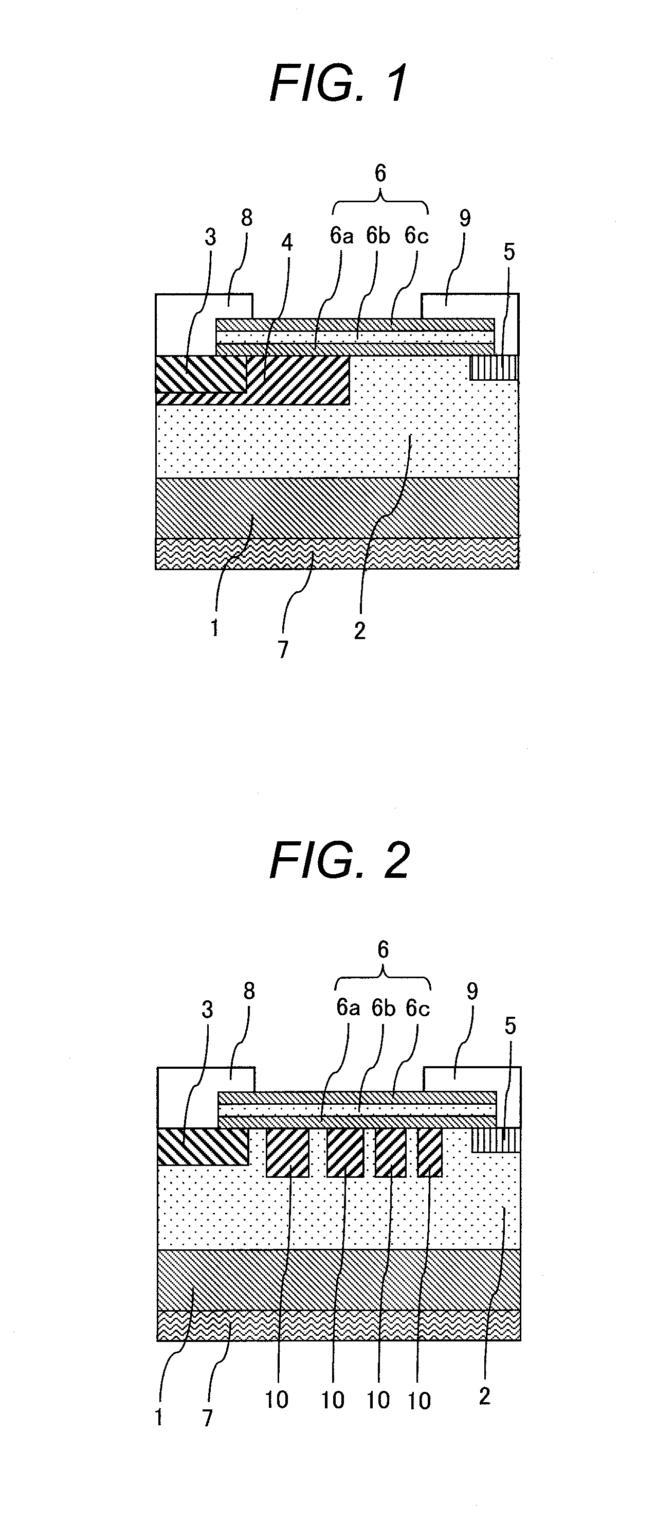
[0040]FIG. 2 is a longitudinal sectional view showing a termination region of an SiC semiconductor device according to another embodiment of the present invention. The second embodiment is described below mainly with respect to points where the present embodiment differs from the first embodiment.

[0041]The present embodiment differs from the first embodiment in that a termination region has the FLR structure. As shown in FIG. 2, a portion of the upper surface of an n− type drift layer 2, interposed between a p+ type guard ring region 3 and an n+ type field stop region 5, is provided with four pieces of p-type FLR regions 10. A portion of the n− type drift layer 2 is interposed between the p+ type guard ring region 3 and the p-type FLR region 10 in close proximity thereto, between two pieces of the p-type FLR regions 10 in close proximity to each other, and between the n+ type field stop region 5 and the p-type FLR region 10 in close proximity thereto, respectively. In other words, t...


PUM


Abstract

With an SiC semiconductor device, the surface of a termination region is covered with a passivation film, and the passivation film is provided with a thermal silicon oxide film which is in contact with the surface of the termination region, a CVD silicon oxide film deposited on the thermal silicon oxide film so as to be in contact with the thermal silicon oxide film, and a CVD silicon oxide film deposed on the CVD silicon oxide film so as to be in contact with the CVD silicon oxide film. By so doing, an electric field applied on the passivation film is relaxed, while production cost is reduced.

Description

CLAIM OF PRIORITY[0001]The present application claims priority from Japanese application serial no. 2014-209618, filed on Oct. 14, 2014, the content of which is hereby incorporated by reference into this application.BACKGROUND OF THE INVENTION[0002]1. Field of the Invention[0003]The invention relates to a semiconductor device using silicon carbide as the semiconductor material thereof, and a method of manufacturing the same.[0004]2. Description of Prior Art[0005]Efforts are being put into research and development of a semiconductor device using silicon carbide (hereinafter referred to “SiC”), as a new semiconductor material, for use in a semiconductor substrate, by substituting for the traditional silicon (hereinafter referred to “Si”), in an attempt to achieve substantial reduction in power loss of a power device where a large current flows there through, while requiring high blocking voltage. Because SiC has a dielectric breakdown electric-field ten times as large as that of Si, S...

Claims


Application Information

Patent Timeline
IPC IPC(8): H01L21/02H01L29/06H01L29/16
CPCH01L21/02529H01L21/02164H01L21/02255H01L21/02271H01L29/1608H01L29/0615H01L21/02236H01L29/6606H01L29/8611H01L29/0619H01L29/0638H01L23/291H01L23/3192
Inventor HASEGAWA, JIROTOYOTA, YOSHIAKI
Owner HITACHI LTD
Why Eureka
Try Eureka