Switching device and switching arrangements for switching at high operating voltage

a high-operational voltage, switching device technology, applied in the direction of pulse automatic control, pulse manipulation, electrical apparatus, etc., can solve the problems of increased costs, inability to use the switching device in those applications, and steps in the switching-on of the serially wired high-voltage switching elements, so as to reduce the loss of transfer

Inactive Publication Date: 2010-02-04
SIEMENS HEALTHCARE GMBH
View PDF3 Cites 5 Cited by
  • Summary
  • Abstract
  • Description
  • Claims
  • Application Information

AI Technical Summary

Benefits of technology

[0018]Alternatively, a capacitor and a serial circuit from the second resistor are connected parallel with the optically triggerable switching element, and the parallel connection is connected with the second main connector of the controllable switching element, as well as via an uncoupling element with the first main connector of the controllable switching element. A node point of the serial circuit including the optically triggerable switching element and the second resistor is connected with a control connector of the controllable switching element. As a result, an intermediate circuit capacitor is made available, from which the energy required for switching the controllable switching element into the conducting state can be made available. Because of this it is possible to do without the resistor located in the switching section, so that transfer losses can be reduced.
[0019]The first self-conducting switching element and / or the at least one second self-conducting switching element may be a JFET (Junction Field Effect Transistor). The first self-conducting switching element and / or the at least one second self-conducting switching element may be a MOSFET, whose gate connector is connected with the source connector by a respective diode. An excess voltage in case of blocking is prevented because of the provision of the diode.

Problems solved by technology

However, the switching device represented in DE 101 35 835 C1 has the disadvantage that switching-on of the serially wired high voltage switching elements takes place in steps (intervals) by the breakdown of the serially wired protective elements.
The switching device cannot be used in those applications in which the simultaneous opening of the switching elements is required.
It is problematical that these active triggering devices are connected to different electrical potentials.
Accordingly, a considerable technical outlay is required, which also leads to increased costs.

Method used


Image

  • Switching device and switching arrangements for switching at high operating voltage
  • Switching device and switching arrangements for switching at high operating voltage
  • Switching device and switching arrangements for switching at high operating voltage

Examples


Embodiment Construction

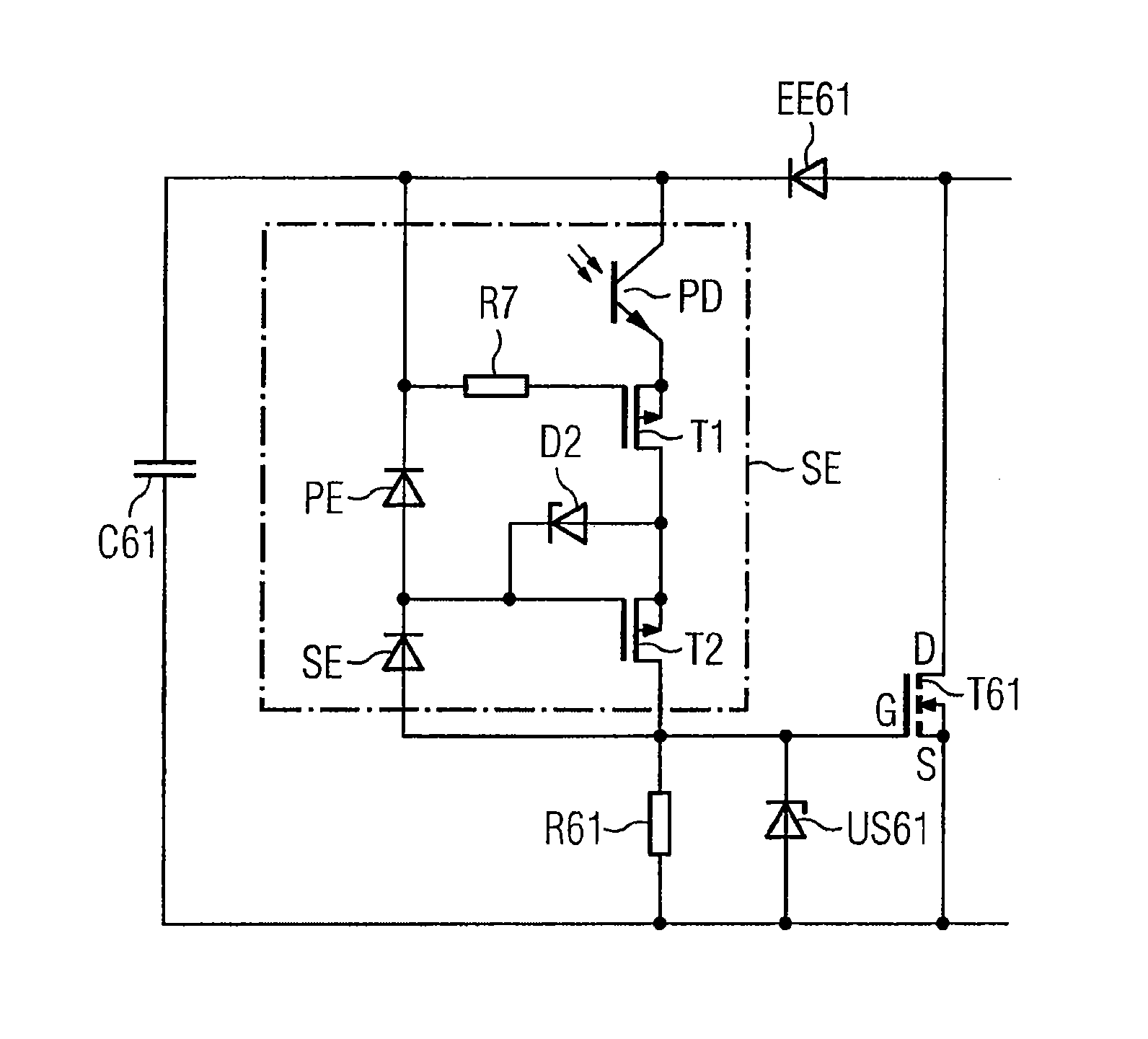
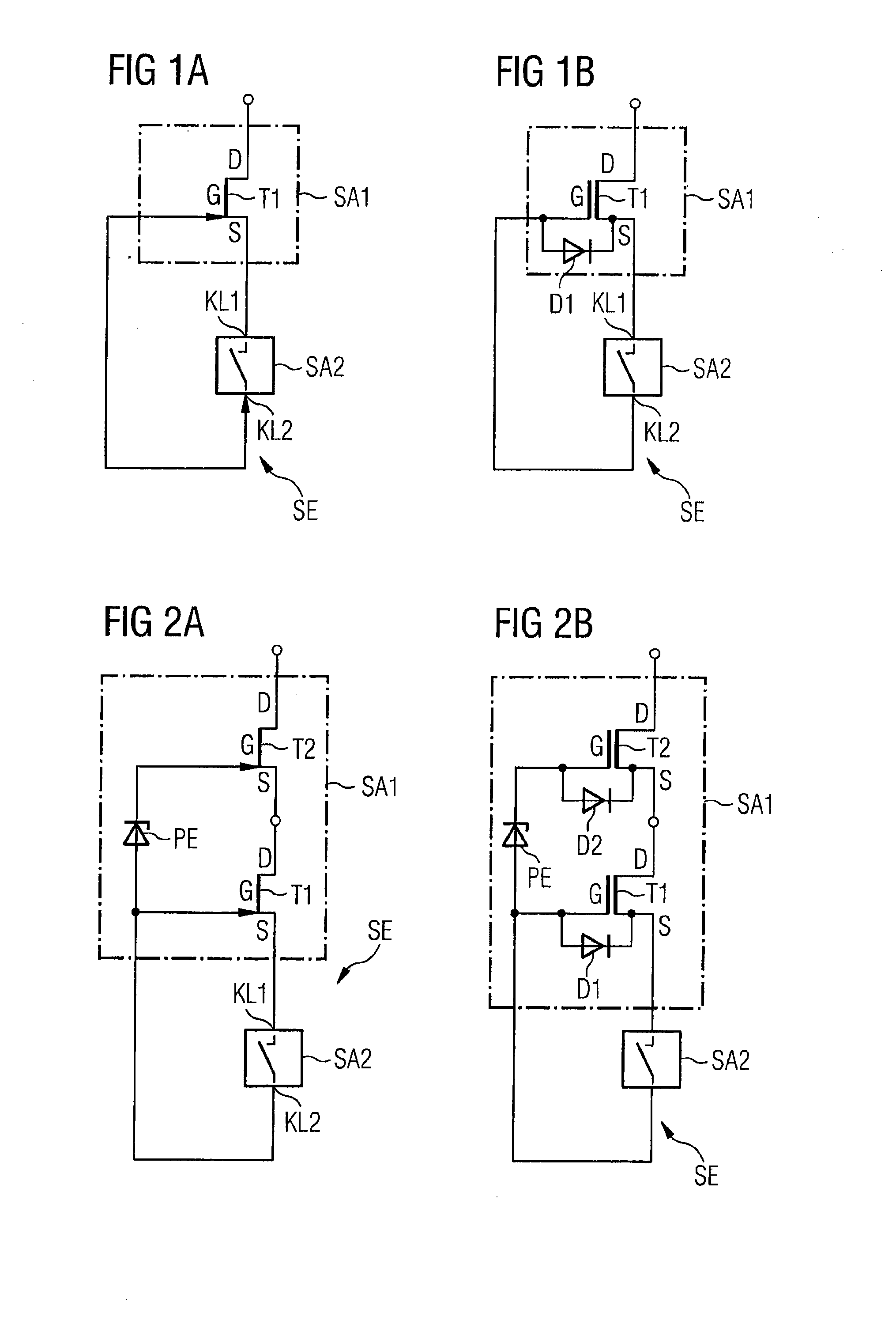
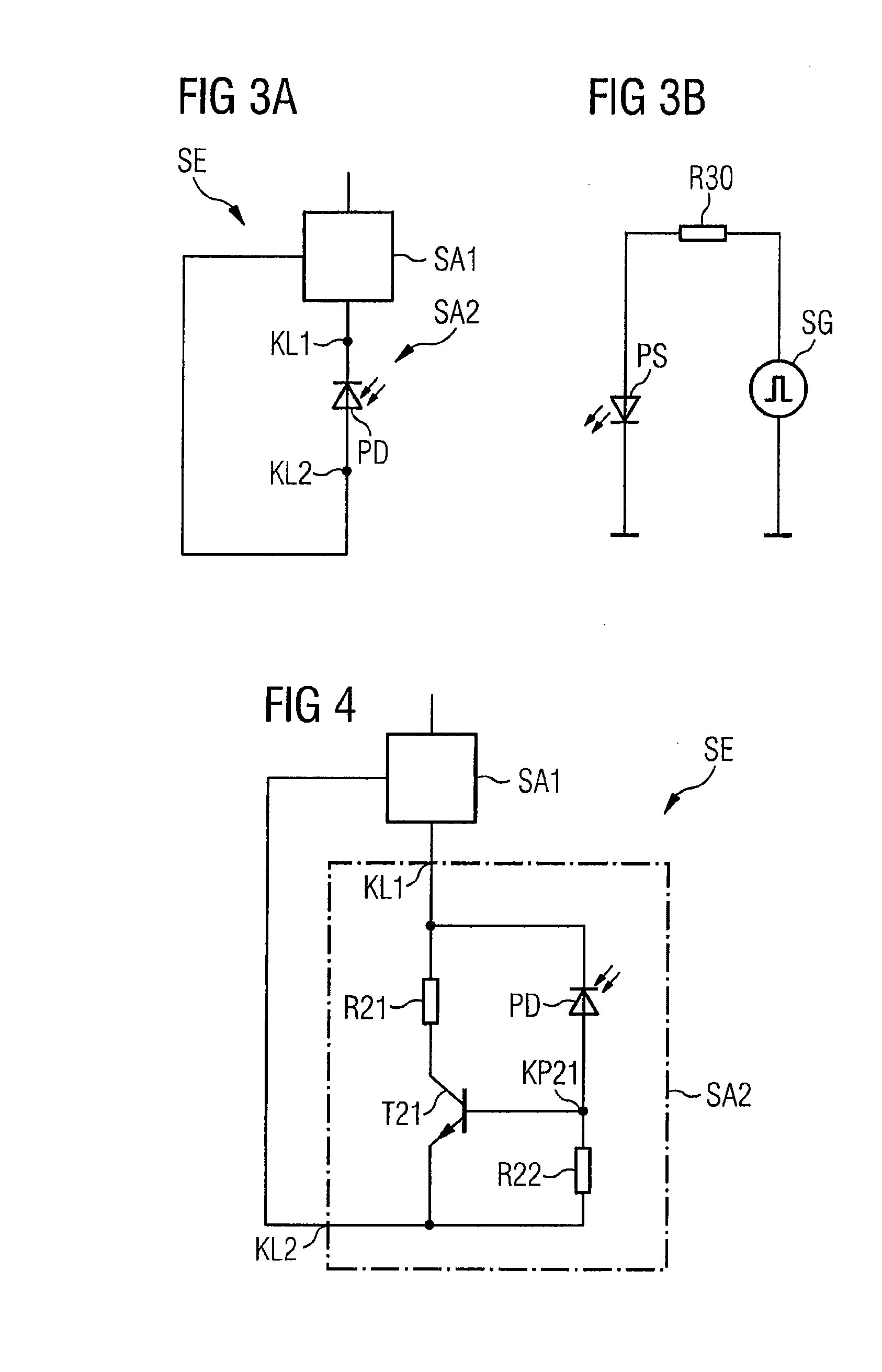
[0035]FIGS. 1A and 1B show a switching arrangement SE. The switching arrangement SE includes a first switching device SA1, which is wired in series with a second switching device SA2.

[0036]The switching device SA1 has a single self-conducting switching element T1, which in FIG. 1A is a JFET. The JFET has a control connector (gate connector), a first main connector (drain connector D) and a second main connector (source connector S). The gate connector G of the JFET T1 is, at the same time, the control connector of the first switching arrangement. The source connector S of the JFET T1 is the second main connector of the switching arrangement. If, as in the exemplary embodiment of FIG. 1A, the first switching arrangement SA1 only has a first switching element, the drain connector D of the JFET forms the first main connector of the first switching arrangement SA1.

[0037]The switching device in FIG. 1B differs from the switching device of FIG. 1A in that the JFET has been replaced by a M...


PUM


Abstract

A switching device for switching a high operating voltage is described. The switching device-includes a first switching arrangement with a first self-conducting switching element), which has a control connector and a first and second main connector for forming a switching section. The switching device may include a second switching arrangement having a first and a second connector for forming a switching section, which is wired serially in respect to the switching section of the first switching arrangement. The second switching arrangement includes an optically triggerable switching element for switching the switching section of the second switching arrangement so it becomes conductive. The second connector of the second switching arrangement is connected with the control connector of the first self-conducting switching element.

Description

[0001]This patent document claims the benefit of DE10 2008 035 075.3 filed Jul. 28, 2008, which is hereby incorporated by reference.BACKGROUND[0002]The present embodiments relate to a switching device for switching a high operating voltage.[0003]DE 101 35 835 C1 discloses a switching device for switching at a high operating voltage. The switching device combines one low voltage (LV) and at least one high voltage (HV) switching element. This type of combining is called cascade switching. The switching device is used for switching a high electric current and is also capable of safely blocking a high operating voltage. The low voltage switching element is a self-blocking metal-oxide-semiconductor field-effect transistor (MOSFET). A number of high voltage switching elements, which are serially wired with respect to each other (i.e., a cascade circuit), is realized in the form of self-conducting blocking layer field effect transistors (JFETs).[0004]The voltage stability of the switching ...

Claims


Application Information

Patent Timeline
Patent Type & Authority Applications(United States)
IPC IPC(8): H03K17/687
CPCH03K17/10H03K17/795H03K17/785H03K17/102
Inventor KOMMA, THOMASSELIGER, NORBERT
Owner SIEMENS HEALTHCARE GMBH
Why Eureka
Try Eureka