Silicon carbide Schottky diode and preparation method thereof

A Schottky diode, silicon carbide technology, applied in semiconductor/solid-state device manufacturing, semiconductor devices, electrical components, etc. The effect of increased pass area, good turn-on characteristics and reverse recovery characteristics, and simple fabrication process

Pending Publication Date: 2018-09-21
GLOBAL POWER TECH CO LTD
View PDF0 Cites 5 Cited by
  • Summary
  • Abstract
  • Description
  • Claims
  • Application Information

AI Technical Summary

Problems solved by technology

However, in the junction barrier Schottky diode, the ion-implanted junction region cannot conduct electricity, so the effectiv

Method used


Image

  • Silicon carbide Schottky diode and preparation method thereof
  • Silicon carbide Schottky diode and preparation method thereof
  • Silicon carbide Schottky diode and preparation method thereof

Examples


Embodiment Construction

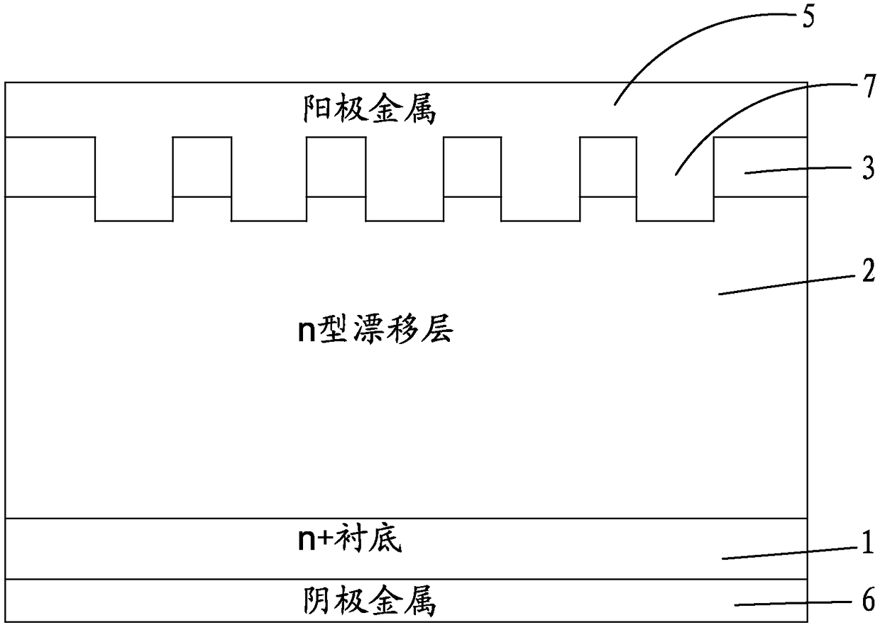
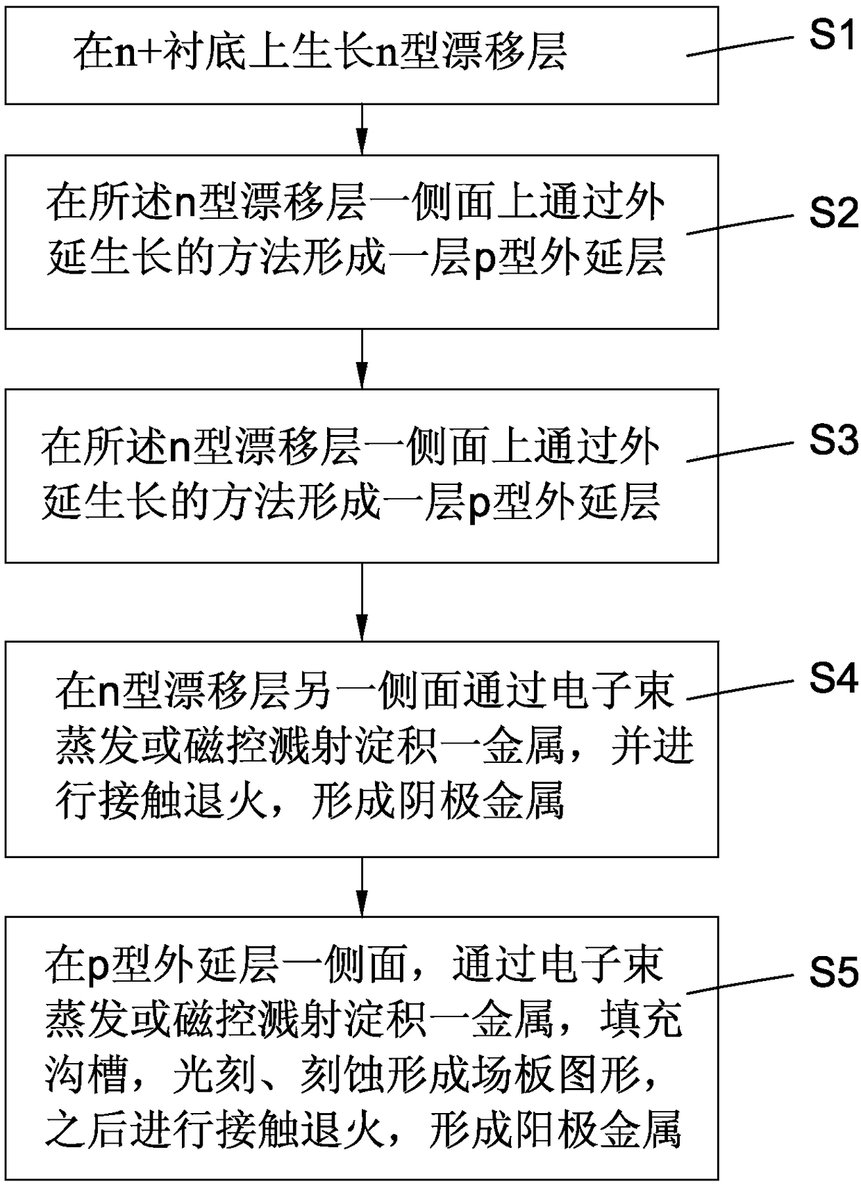
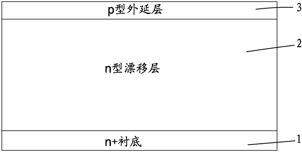
[0034] see figure 1 As shown, the silicon carbide Schottky diode of the present invention includes an anode metal 5, a p-type epitaxial layer 3, an n-type drift layer 2, an n+ substrate 1, and a cathode metal 6 arranged in sequence from top to bottom. Layer 3 is provided with a plurality of grooves 4, the grooves 4 pass through the p-type epitaxial layer 3, and a plurality of protrusions 7 are arranged on one side of the anode metal 5, and the protrusions 7 are connected to the grooves. slot 4, the thickness of the n-type epitaxial layer is 5um to 200um, and the doping concentration is 1×10 14 cm -3 to 1×10 16 cm -3 , the thickness of the p-type epitaxial layer 3 is 0.3um to 1.5um, and the doping concentration is greater than or equal to 1×10 18 cm -3 , the width of the trench 4 is 1um to 8um, the depth of the trench 4 is greater than the thickness of the p-type epitaxial layer 3, the depth of the trench 4 is 0.8um to 3um, and the anode metal 5 is Al or Ti, the cathode m...


PUM

PropertyMeasurementUnit
Thicknessaaaaaaaaaa
Thicknessaaaaaaaaaa
Doping concentrationaaaaaaaaaa

Abstract

The present invention provides a silicon carbide Schottky diode comprising anode metal, a p-type epitaxial layer, an n-type drift layer, an n+ substrate, and cathode metal which are disposed successively from top to bottom, wherein the p-type epitaxial layer is provided a plurality of trenches passing through the p-type epitaxial layer; and a side of the anode metal is provided with a plurality ofprotrusions matching the trenches. The present invention also provides a preparation method of the silicon carbide Schottky diode. The anode contact area of the Schottky diode is increased and the on-resistance of a device is reduced by using the trench structure on the basis of ensuring the blocking voltage.

Description

technical field [0001] The invention relates to a silicon carbide Schottky diode and a preparation method thereof. Background technique [0002] Silicon carbide is an emerging third-generation semiconductor material with good physical and electrical properties. With its advantages such as wide band gap, high thermal conductivity and high critical electric field, it has become the best choice for making high temperature, high power and high frequency semiconductor devices. Ideal material. Silicon carbide Schottky diodes are the earliest commercialized silicon carbide semiconductor devices, featuring short reverse recovery time and extremely small reverse recovery charge. Common commercial Schottky diodes are Schottky Barrier Diodes and Junction Barrier Schottky Diodes. [0003] The Schottky barrier diode uses the gold half-contact barrier to achieve reverse blocking; while the junction barrier Schottky diode uses the space charge region of the reverse-biased PN junction to ...

Claims


Application Information

Patent Timeline
IPC IPC(8): H01L29/872H01L21/329H01L29/24
CPCH01L29/8725H01L29/24H01L29/6606
Inventor 陈彤
Owner GLOBAL POWER TECH CO LTD
Why Eureka
Try Eureka