Check patentability & draft patents in minutes with Patsnap Eureka AI!

Connecting structure and connecting method for PCB

A PCB board and connection structure technology, which is applied in the direction of electrical connection of printed components, printed circuit components, and assembly of printed circuits with electrical components, can solve the problems of increased device cost, poor reliability, and occupancy, and achieve PCB board area reduction , increase flexibility and reduce cost

Active Publication Date: 2011-06-29
GUANGDONG DAPU TELECOM TECH CO LTD
View PDF2 Cites 3 Cited by
  • Summary
  • Abstract
  • Description
  • Claims
  • Application Information

AI Technical Summary

Problems solved by technology

Another commonly used process is to use a connector to connect two boards, but there are many disadvantages in the way of using a connector. The smaller connector is more expensive, which increases the cost of the device.
In addition, due to the use of connectors, the reliability is not as good as direct welding
Usually a connector is used, which can only maintain the electrical signal connection of the two boards, and cannot be used for structural positioning. If you need to fix the superimposed PCB board, you need to install additional positioning devices
Also, the use of connectors will take up more PCB wiring area

Method used


Image

  • Connecting structure and connecting method for PCB
  • Connecting structure and connecting method for PCB
  • Connecting structure and connecting method for PCB

Examples


Embodiment Construction

[0021] Embodiments of the present invention will now be described with reference to the accompanying drawings, in which like reference numerals represent like elements.

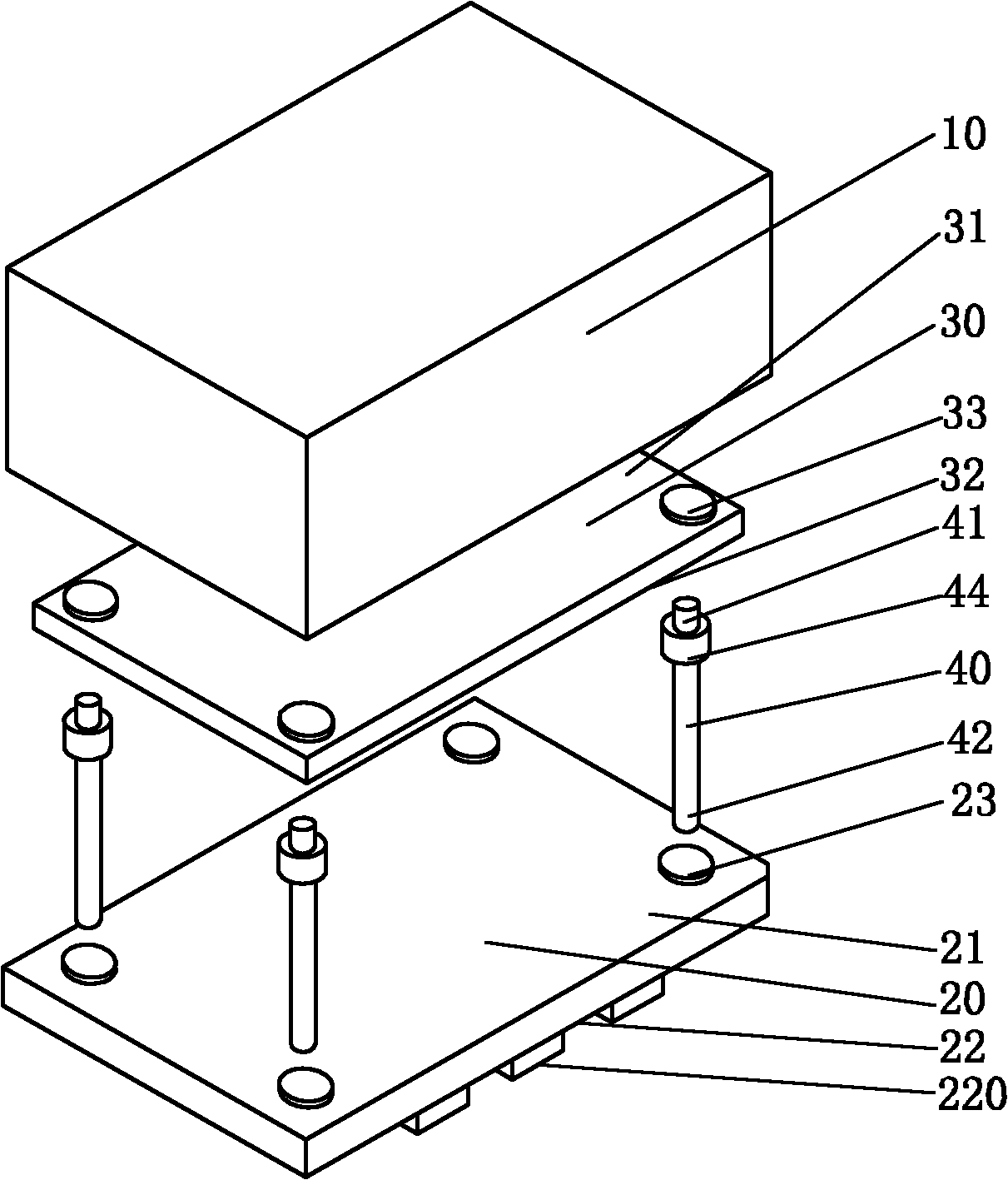
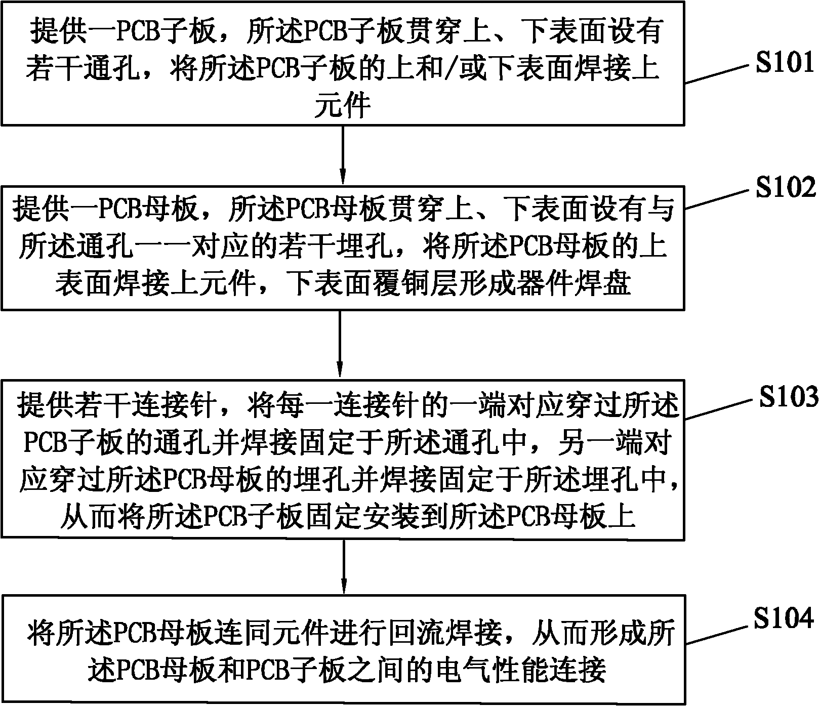
[0022] First please refer to figure 1 , The connection structure of the PCB board of the present invention includes a metal casing 10 , a PCB motherboard 20 , a PCB daughter board 30 and a plurality of connection pins 40 . The upper surface 21 of the PCB motherboard 20 is the component welding surface, the lower surface 22 of the PCB motherboard 20 forms the device pads 220, and the device pads 220 are the function lead-out pads of the device. The lower surface 22 of the board 20 is made of a copper clad layer and is used for soldering on the PCB board of the application product; and the PCB motherboard 20 is provided with a number of buried holes 23 through the upper surface 21 and the lower surface 22 . The upper surface 31 and the lower surface 32 of the PCB sub-board 30 are both component welding surface...


PUM


Abstract

The invention discloses a connecting structure for a PCB (Printed Circuit Board), which comprises a PCB mother board and a PCB daughter board, wherein the upper surface of the PCB mother board is an element welding surface, the lower surface of the PCB mother board forms a device welding pad, and four buried holes penetrating the upper and the lower surfaces of the PCB mother board are formed on the PCB mother board; and at least one of the upper surface and the lower surface of the PCB daughter board is an element welding surface, and four through holes in one-to-one correspondence to the buried holes of the PCB mother board and penetrating the upper and the lower surfaces of the PCB daughter board are formed on the PCB daughter board. The connecting structure further comprises four connecting needles, wherein one end of each connecting needle correspondingly penetrates one through hole and is fixedly welded in the through hole, and the other end of the connecting needle correspondingly penetrates one buried hole and is fixedly welded in the buried hole, so that the PCB daughter board is fixedly mounted on the PCB mother board, and the PCB daughter board and the PCB mother board are electrically connected. Each connection needle is provided with a spacing ring sleeved on one end welded with the PCB daughter board, so that the height of each connection needle welded with the PCB daughter board is accordance. The through holes and buried holes are all uniformly distributed on the periphery of the PCB daughter substrate and the PCB mother board. The invention further discloses a connecting method for the PCB.

Description

technical field [0001] The invention relates to a PCB circuit board, and more particularly to a PCB board connection structure and connection method. Background technique [0002] With the increasing requirements for miniaturization of electronic products, the size of the PCB board area has become a very important issue. [0003] For manufacturers who use PCB boards to make surface mount devices, the usual practice is to use the bottom copper clad layer of the PCB to make device pads, and the top copper clad layer to wire and place components. In this process, the PCB has only one component surface that can be placed. Place components. For devices with more complex functions, since there is only one surface for placing components, the number of devices that can be accommodated cannot meet the requirements. The only way to expand the area of ​​the PCB is to increase the volume of the device; [0004] Due to customer requirements and product appearance limitations, the method...

Claims


Application Information

Patent Timeline
Patent Type & Authority Applications(China)
IPC IPC(8): H05K1/02H05K1/11H05K3/34H05K3/36
Inventor 刘朝胜
Owner GUANGDONG DAPU TELECOM TECH CO LTD
Features
  • R&D
  • Intellectual Property
  • Life Sciences
  • Materials
  • Tech Scout
  • Unparalleled Data Quality
  • Higher Quality Content
  • 60% Fewer Hallucinations
Learn More