

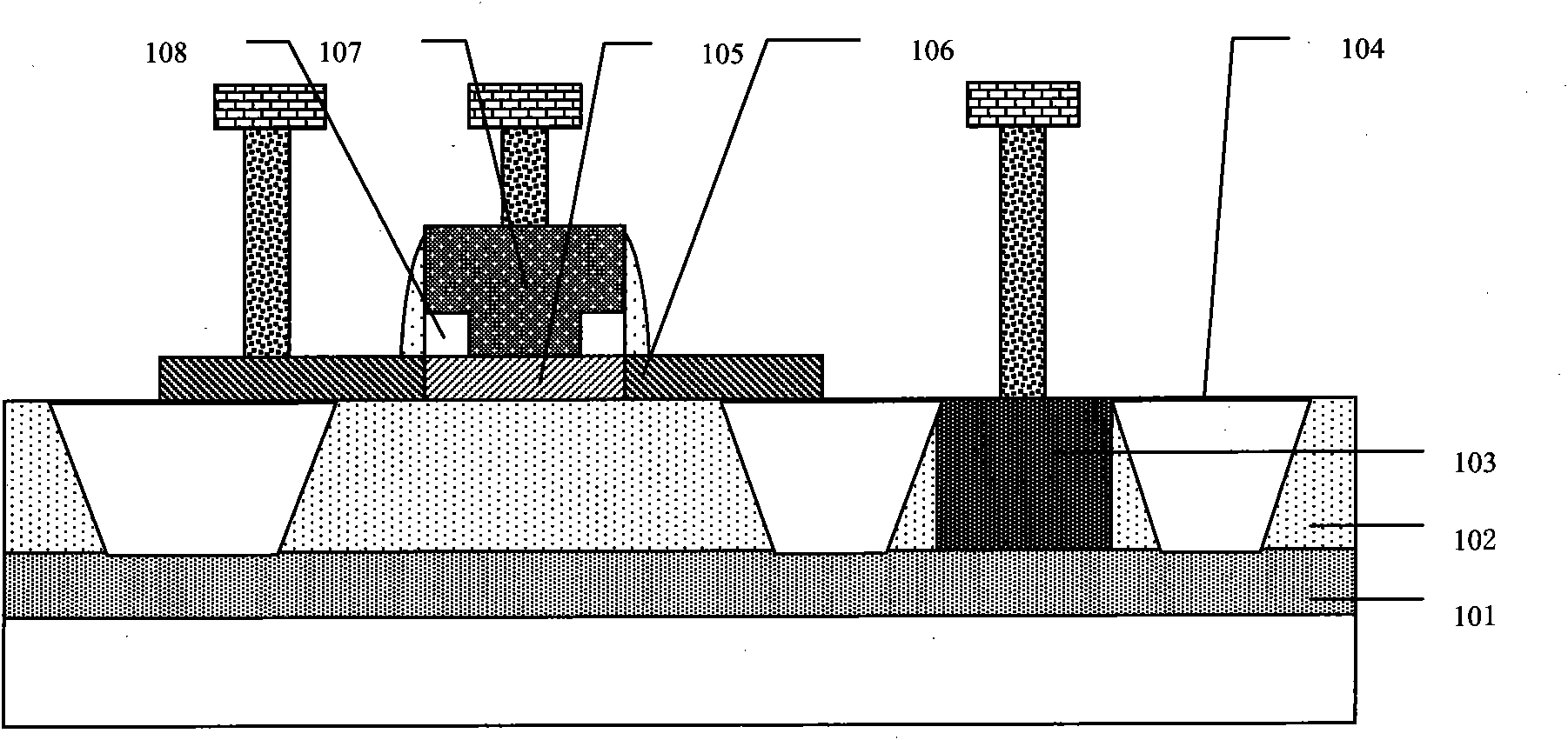
Electrode lead-out structure in STI process
An electrode extraction, shallow trench technology, applied in circuits, electrical components, electrical solid devices, etc., can solve the problems of large collector parasitic capacitance and large area, and achieve reduced parasitic capacitance, reduced device area, The effect of increasing the eigenfrequency
- Summary
- Abstract
- Description
- Claims
- Application Information
AI Technical Summary
Problems solved by technology
Method used
Image

Examples
Embodiment Construction
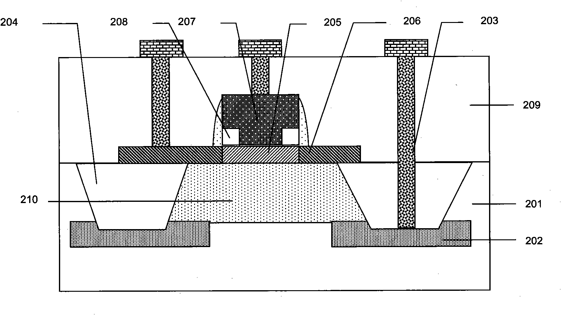
[0017] Such as figure 2 As shown, it is a structural diagram of the first embodiment of the present invention, the active region 201 is isolated by a shallow trench 204, and includes a collector region 210, a base region and an emitter region 207, wherein the collector region 210 corresponds to the The doped region one. The base region is composed of an epitaxial layer of a second conductivity type formed on the collector region 210, including an intrinsic base region 205 and an extrinsic base region 206, and the intrinsic base region 205 and the collector region 210, and the base is drawn out by making a metal contact on the outer base region 206. The emitter region 207 is formed of polysilicon of the first conductivity type formed on the base region, and the emitter is drawn out by direct metal contact on the polysilicon. The collector region 210 is composed of an impurity ion-implanted layer with the first conductivity type, and the bottom is connected to a high-concentr...
PUM
 Abstract
Description
Claims
Application Information