Unlock instant, AI-driven research and patent intelligence for your innovation.
Ultrathin packaging structure and packaging method of image sensing chip
What is Al technical title?
Al technical title is built by PatSnap Al team. It summarizes the technical point description of the patent document.
A technology of image sensing and packaging structure, which is applied in radiation control devices, electrical components, electric solid devices, etc.
Inactive Publication Date: 2011-07-06
KUSN WEALTH DYNASTY ELECTRIC
View PDF0 Cites 19 Cited by
Summary
Abstract
Description
Claims
Application Information
AI Technical Summary
This helps you quickly interpret patents by identifying the three key elements:
Problems solved by technology
Method used
Benefits of technology
Problems solved by technology
It can be seen from the figure that the thickness after docking is relatively thick, which is directly the thickness of the package structure 300 plus the thickness of the second body 30, and the trend of light, thin and short in the existing technology can no longer meet the requirements
Method used
Image
Click on the blue label to locate the original text in one second.
Reading with bidirectional positioning of images and text.
Examples
Embodiment 1
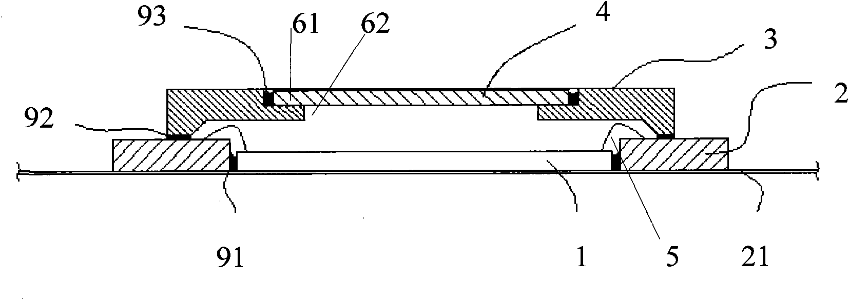
[0041] Such as Figure 1-3 As shown, the packaging process of the ultra-thin packaging structure of the image sensing chip provided by the first preferred embodiment of the present invention includes the following steps:
[0042] The first step: stick the film 21 on the lower surface 82 of the substrate 2, and apply glue 91 around the hollow part of the substrate 2;
[0043] Step 2: Put the image sensing chip 1 into the hollowed out part of the substrate 2, cure the glue 91, and fix the substrate 2 and the image sensing chip 1 together.
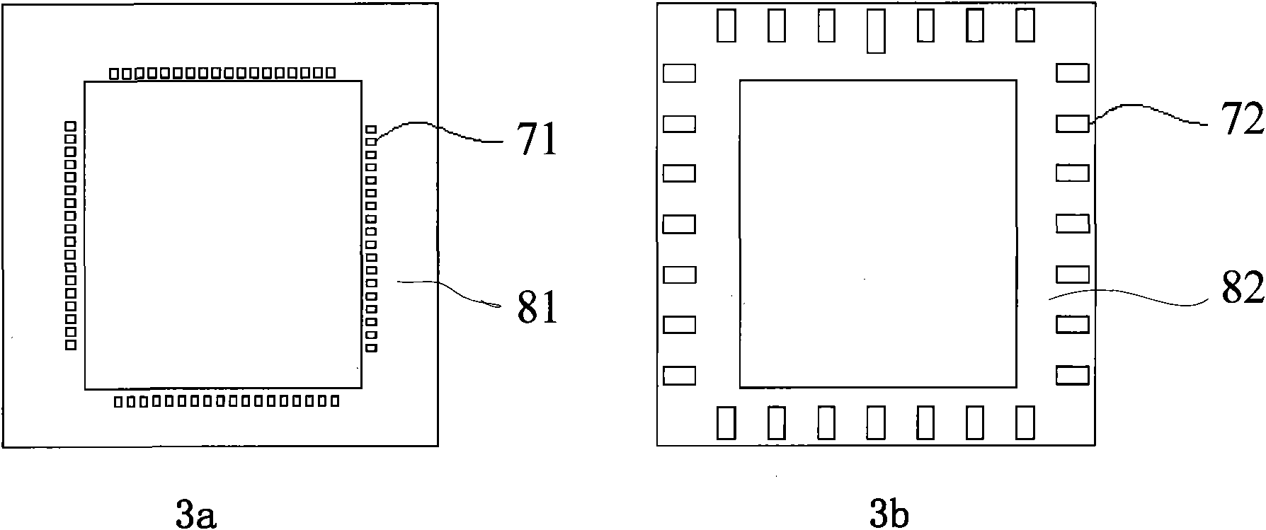
[0044] Step 3: Connect the pads 71 on the upper surface 81 to the pads on the image sensing chip 1 with wires 5;
[0045] Step 4: Apply glue 92 around the upper surface 81 of the substrate 2, place the bracket 3 on top of the glue 92, then cure the glue 92, and fix the bracket and the substrate together;
[0046] Step 5: Apply glue around the first step 61 of the bracket 3, put the light-transmitting glass 4 on the glue in the first step fo...
Embodiment 2
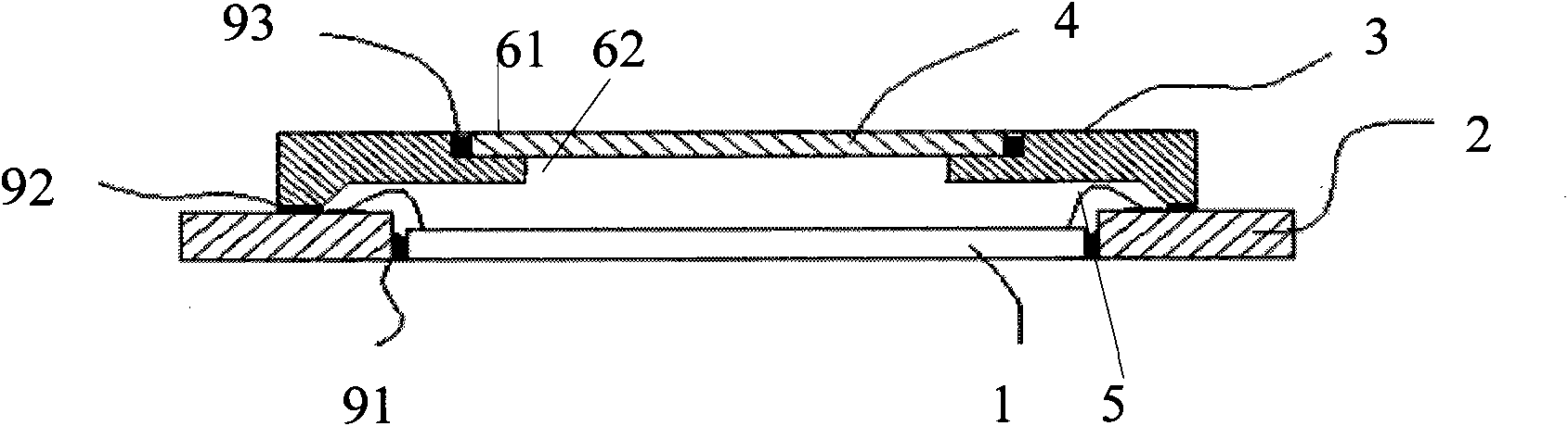
[0049] Such as Figure 3-4 As shown, the packaging process of the ultra-thin packaging structure of the image sensing chip provided by the second preferred embodiment of the present invention includes the following steps:
[0050] Step 1: stick the film 21 on the lower surface 82 of the substrate 2, and then put the image sensing chip 1 into the hollow part of the substrate 2 and stick it together with the film 21;
[0051] Step 2: Connect the pads 71 on the upper surface 81 to the pads on the image sensing chip 1 with wires 5;
[0052] Step 3: Use glue 94 to apply glue around the hollowed-out part of the substrate 2, including the connection between the image sensor chip 1 and the substrate 2 and the connection between the support 3 and the upper surface 81 of the substrate. Put it on the glue on the upper surface 81 of the substrate, then cure the glue, and fix the substrate 2, the image sensing chip 1 and the bracket 3 together;
[0053] Step 4: Apply glue around the fi...
PUM
Abstract
The invention discloses an ultrathin packaging structure of an image sensingchip, comprising a base plate, an image sensingchip, a support and a light transmission layer, wherein the base plate comprises an upper surface and a lower surface and is hollow in the middle part; a welding pad for connection chips is arranged around the hollow part of the upper surface; a welding pad for subsequent welding is arranged around lower surface; the image sensingchip is arranged at the hollow part of the base plate and smaller than the hollow part of the base plate to ensure that the image sensing chip can be totally placed in the base plate; the welding pad of the chip and the welding pad on the base plate are connected through wires; the support is of a frame structure; the lower surface of the support is connected with the upper surface of the base plate; stepped grooves are arranged on the upper surface of the support; and the light transmission layer is a piece of light transmission glass which is connected in the grooves of the support by utilizing glue. The invention also discloses a packaging method of the image sensing chip with the ultrathin packaging structure. The ultrathin packaging structure of the image sensing chip can be applied to ultrathin electronic products.
Description
technical field [0001] The invention relates to a packaging structure of a chip, in particular to a packaging structure of an image sensing chip; the invention also relates to a packaging method of the packaging structure. Background technique [0002] In the semiconductor industry, the production of integrated circuits (IC) is mainly divided into three stages: manufacturing of wafers, manufacturing of integrated circuits, and packaging of integrated circuits. Among them, the bare chip (die) is completed through steps such as chip fabrication, circuit design, photomask fabrication, and wafer saw. Each bare chip formed by chip dicing can be coated with a molding compound after being electrically connected to external signals through the contacts on the bare chip. The purpose of its packaging is to prevent the bare chip from being affected by moisture, heat, and noise, and to provide a medium for electrical connection between the bare chip and the external circuit, thus compl...
Claims
Application Information
Patent Timeline
Application Date:The date an application was filed.
Publication Date:The date a patent or application was officially published.
First Publication Date:The earliest publication date of a patent with the same application number.
Issue Date:Publication date of the patent grant document.
PCT Entry Date:The Entry date of PCT National Phase.
Estimated Expiry Date:The statutory expiry date of a patent right according to the Patent Law, and it is the longest term of protection that the patent right can achieve without the termination of the patent right due to other reasons(Term extension factor has been taken into account ).
Invalid Date:Actual expiry date is based on effective date or publication date of legal transaction data of invalid patent.
