Template and method of making high aspect ratio template for lithography and use of the template for perforating a substrate at nanoscale

A technology of aspect ratio and template, which is applied in the field of perforation of nano-scale substrates, can solve the problems of environmental protection

Active Publication Date: 2011-07-06
SMOLTEK AB
View PDF5 Cites 6 Cited by
  • Summary
  • Abstract
  • Description
  • Claims
  • Application Information

AI Technical Summary

Problems solved by technology

[0014] Generation of large amounts of waste: Today's technology is limited to reusing substrates or re-preparing templates on the same substrate, thus creating a large amount of waste by discarding irreparable substrates and stamps, thus not being environmentally friendly

Method used


Image

  • Template and method of making high aspect ratio template for lithography and use of the template for perforating a substrate at nanoscale
  • Template and method of making high aspect ratio template for lithography and use of the template for perforating a substrate at nanoscale
  • Template and method of making high aspect ratio template for lithography and use of the template for perforating a substrate at nanoscale

Examples


Embodiment Construction

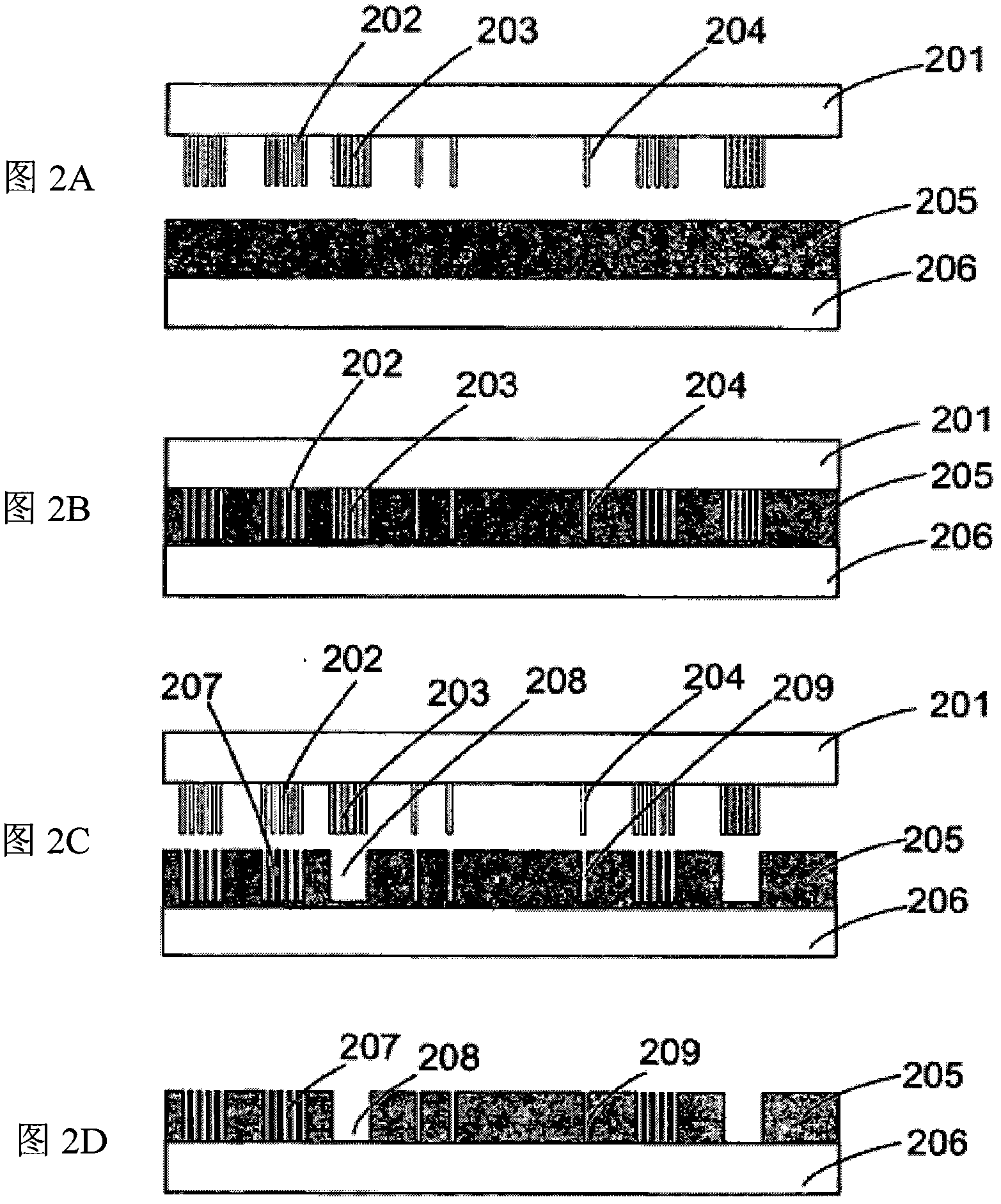
[0038] According to the template 201 of the present invention such as figure 2 As shown in A. Nanostructures 204 with independent vertical alignment. Also visible on the stamp is an array 202 of vertically aligned nanostructures and a cluster of grown nanostructures 203 . A polymer / barrier 205 is deposited on the underlying substrate / wafer 206 . The substrate may contain multiple layers.

[0039] figure 2 In B a template 201 according to the invention is pressed against a polymer layer 205 on a wafer 206 . The wafer and barrier are heated above the glass transition temperature of the polymer. After cooling the template is lifted, leaving depressions 207, 208 and 209 in the barrier layer. Depending on the localization of the nanostructures, different types of results can occur in the imprinted polymer layer. for figure 2 Individual fibers 204 and finely spaced array 202 shown in A, each fiber will give depressions 207 and 209 in the polymer. For a very fine pitch array...


PUM


Abstract

Template and method of making high aspect ratio template, stamp, and imprinting at nanoscale using nanostructures for the purpose of lithography, and to the use of the template to create perforations on materials and products.

Description

technical field [0001] The invention relates to a template, a method for forming a high aspect ratio template for photolithography, and the application of the template in perforating a nanoscale substrate. Background technique [0002] To date, the miniaturization of CMOS devices has followed a trend commonly known as Moore's Law, in which the size of electronic components shrinks by half every two years. The International Technology Roadmap for Semiconductors (ITRS) has established a projected growth curve based on this model. The ensuing demands for speed, high integration, high performance, and low production cost in terms of this rate of progress are severe. As a result, problems associated with the need to reduce feature size have escalated, and among these problems, photolithographic transfer of patterns at the nanoscale is prominent. Therefore, there is a need to find alternatives to these problems that will ultimately hinder the development of silicon technology in...

Claims


Application Information

Patent Timeline
Patent Type & Authority Applications(China)
IPC IPC(8): G03F7/00
CPCB82Y10/00G03F7/0002B82Y40/00Y10S977/932
Inventor 阿明・萨利姆・穆罕默德大卫・布鲁德乔纳斯・贝尔格穆罕默德・沙菲奎尔・卡比尔文森特・代马雷
Owner SMOLTEK AB
Why Eureka
Try Eureka