Differential structure single-gate memory applicable to ultra high frequency (UHF) radio frequency identification device (RFID) passive label chip

A differential structure and memory technology, applied in the field of microelectronics, can solve the problems of incompatibility with CMOS technology, affect the popularization and application of RFID tags, and high cost, and achieve the effect of reducing technology development cycle, shortening time to market, and improving reliability

Inactive Publication Date: 2012-12-05
XIDIAN UNIV
View PDF0 Cites 0 Cited by
  • Summary
  • Abstract
  • Description
  • Claims
  • Application Information

AI Technical Summary

Problems solved by technology

But none of them are compatible with the standard CMOS process, and require additional special process manufacturing, which greatly increases the manufacturing cost of RFID tags
At present, the main bottleneck restricting the promotion of RFID technology is the high cost. All major manufacturers are trying to reduce the manufacturing cost of RFID tag chips in order to further expand the market of RFID technology. However, the above-mentioned memories are not suitable for RFID tags, which affects the RFID technology. Promotional application of tags

Method used


Image

  • Differential structure single-gate memory applicable to ultra high frequency (UHF) radio frequency identification device (RFID) passive label chip
  • Differential structure single-gate memory applicable to ultra high frequency (UHF) radio frequency identification device (RFID) passive label chip
  • Differential structure single-gate memory applicable to ultra high frequency (UHF) radio frequency identification device (RFID) passive label chip

Examples


Embodiment Construction

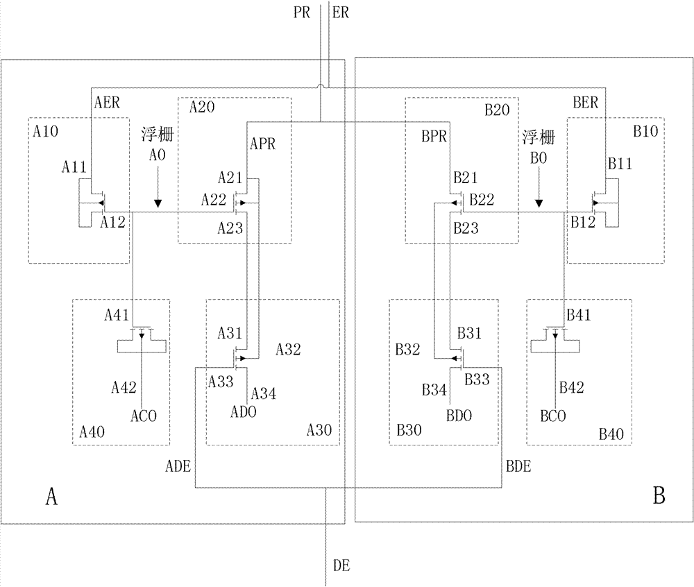
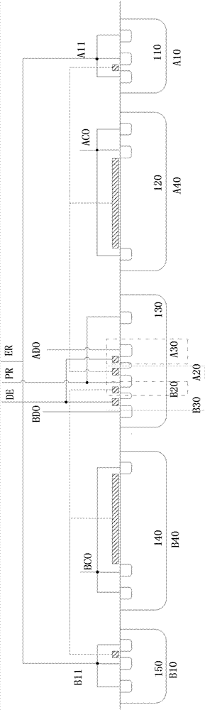
[0021] Hereinafter, a single-gate semiconductor memory according to an embodiment of the present invention will be described in detail with reference to the accompanying drawings.

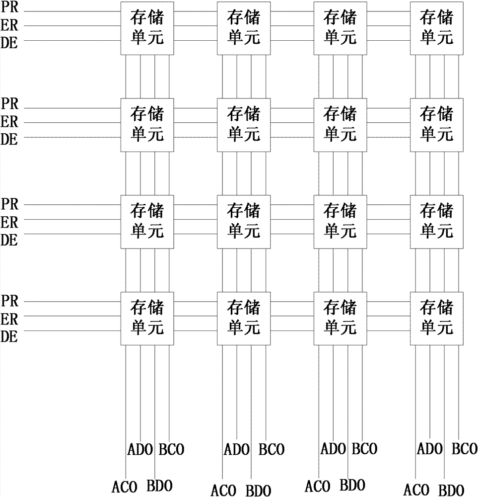
[0022] refer to figure 1 , the present invention is made up of a plurality of identical storage units, and the storage unit of this example is 16, and namely memory capacity is 16, but not limited to 16, and the actual number of storage units is determined according to the required capacity. from figure 1 It can be seen that in each row, the programming terminals PR of all memory cells are connected in parallel, the erasure terminals ER of all memory cells are connected in parallel, and the decoding terminals DE of all memory cells are connected in parallel; in each column , the data output terminals ADO of all storage units are connected in parallel, the data output terminals BDO of all storage units are connected in parallel, the coupling terminals ACO of all storage units are connected in paral...


PUM


Abstract

The invention discloses a differential structure single-gate non-volatile memory for an ultra high frequency (UHF) radio frequency identification device (RFID) passive label chip, which mainly solves the problem that the conventional double-gate memory is not compatible with a standard complementary metal oxide semiconductor (CMOS) process. The differential structure single-gate non-volatile memory comprises a plurality of identical memory units; and each memory unit comprises two identical modules, and each module comprises a coupled transistor, a programming transistor, an erasing transistor, a decoding transistor, a coupled terminal, a programming terminal, an erasing terminal, a decoding terminal and a data output terminal. Gates of the coupled transistor, the programming transistor, and the erasing transistor in each module are connected in parallel and then are used as a floating gate; the programming terminals of the two modules are connected and then are used as the programming terminal (PR) of the memory unit; and the erasing terminals of the two modules are connected and then are used as the erasing terminal (ER) of the memory unit, and the decoding terminals of the two modules are connected and are used as the decoding terminal (DE) of the memory unit. The differential structure single-gate non-volatile memory is compatible with the standard CMOS technology and has the advantages of low cost and high reliability.

Description

technical field [0001] The invention belongs to the technical field of microelectronics and relates to the storage technology of semiconductor integrated circuits, in particular to a differential structure single-gate memory which is suitable for ultra-high frequency radio frequency identification (UHF) RFID tags and is compatible with standard CMOS technology. Background technique [0002] The trend in the automation industry is moving towards high-speed and real-time recognition. Realizing continuous recognition and monitoring requires a further increase in precision. This kind of real-time recognition is often referred to as ambient intelligence. One of the technologies that makes this workable concept is known as radio frequency identification (RFID). It is a non-contact automatic identification technology, which automatically identifies the target object and obtains relevant data through radio frequency signals, without manual intervention, and can work in various harsh...

Claims


Application Information

Patent Timeline
Patent Type & Authority Patents(China)
IPC IPC(8): H03K19/094
Inventor 庄奕琪李小明郎卫义吴赞进刘伟峰
Owner XIDIAN UNIV
Why Eureka
Try Eureka