Method for plating silver on front side of silicon wafer

A silicon wafer, silver plating technology, applied in the direction of electrical components, semiconductor/solid-state device manufacturing, circuits, etc., can solve the problem that the silver film cannot be etched to form a pattern, etc.

Inactive Publication Date: 2011-07-20
SHANGHAI HUA HONG NEC ELECTRONICS
View PDF0 Cites 9 Cited by
  • Summary
  • Abstract
  • Description
  • Claims
  • Application Information

AI Technical Summary

Problems solved by technology

But thin silver films cannot be patterned by etching like other metals

Method used


Image

  • Method for plating silver on front side of silicon wafer
  • Method for plating silver on front side of silicon wafer
  • Method for plating silver on front side of silicon wafer

Examples


Embodiment Construction

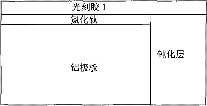
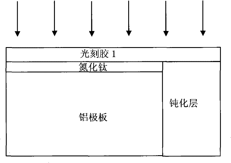
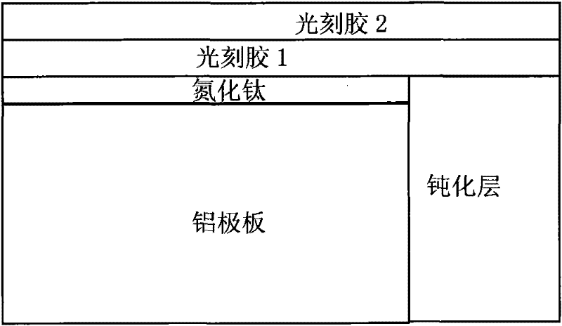
[0009] Figure 9 For the method of silver plating on the front side of the silicon chip of the present invention, the application of the method of the present invention in CLIP Bonding (clip welding) packaging technology as an example will be specifically described below.

[0010] On the surface of the wafer where all processes have been completed, the photoresist is coated twice for exposure, twice and developed once to form an inverted trapezoidal photoresist pattern. Specifically, the photoresist coating is carried out first, and then the entire silicon wafer is exposed without using a photolithography mask (called blind exposure); then the photoresist is coated again, and then the photolithography mask is used for the second exposure. Secondary exposure; develop at last, make the remaining photoresist pattern be an inverted trapezoid (see Figure 1 to Figure 5 , Figure 5 The photoresists in include photoresist 1 and photoresist 2). The thickness of the photoresist coat...


PUM


Abstract

The invention discloses a method for plating silver on the front side of a silicon wafer, which comprises the following steps of: coating photoresist on the front side of the silicon wafer for the first time, and performing exposure on the full silicon wafer; coating the photoresist for the second time, and performing the exposure for the second time by using a photoetching mask; developing, so that the retained photoresist forms an inverted trapezoid graph; depositing the silver on the silicon wafer by an evaporation coating technology, wherein the thickness of the silver is less than that of the retained photoresist; laminating on the silicon wafer and stripping by a laminating and film stripping technology, so that the silver on the photoresist is stripped with a film; and removing the residual photoresist.

Description

technical field [0001] The invention relates to a method for plating silver on the front side of a silicon chip in a chip package. Background technique [0002] In semiconductor integrated circuits, in the chip manufacturing required by typical power MOS transistor packaging technology, it is only necessary to plate silver after thinning the back of the silicon wafer. However, the silicon chip in the CLIP Bonding packaging technology needs to be silver-plated not only on the back side, but also on the front side. Since the front side of the silicon chip is the working area of ​​the device, the plated silver film must be isolated according to the working area of ​​the device. But silver films cannot be patterned by etching like other metals. Contents of the invention [0003] The technical problem to be solved by the present invention is to provide a method for plating silver on the front side of the silicon chip, which can form the desired silver pattern on the front side...

Claims


Application Information

Patent Timeline
Patent Type & Authority Applications(China)
IPC IPC(8): H01L21/60G03F7/26
Inventor 陈冲魏炜殷建斐
Owner SHANGHAI HUA HONG NEC ELECTRONICS
Why Eureka
Try Eureka