Through hole processing method

A processing method and high aspect ratio process technology, applied in the field of semiconductor manufacturing and packaging, can solve problems such as difficulty in conformal coverage of copper barrier layer and copper seed layer, affecting TSV interconnect characteristics, and difficulty in insulating layer technology, and achieve reduction The possibility of failure of small TSV devices, the effect of improving conformal coverage and reducing difficulty

Active Publication Date: 2011-07-20
SHANGHAI INTEGRATED CIRCUIT RES & DEV CENT +1
View PDF4 Cites 13 Cited by
  • Summary
  • Abstract
  • Description
  • Claims
  • Application Information

AI Technical Summary

Problems solved by technology

This will make the subsequent process of forming an insulating layer on the sidewall of the via hole quite difficult.
In addition, it will also bring difficulties to the conformal coverage of the subsequent formation of copper barrier layer and copper seed layer
This will easily affect the interconnection characteristics of the entire TSV, thereby causing the entire device to fail

Method used


Image

  • Through hole processing method
  • Through hole processing method
  • Through hole processing method

Examples


Embodiment Construction

[0029] In order to make the content of the present invention clearer and easier to understand, the content of the present invention will be described in detail below in conjunction with specific embodiments and accompanying drawings.

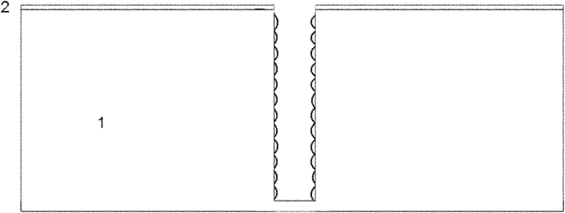
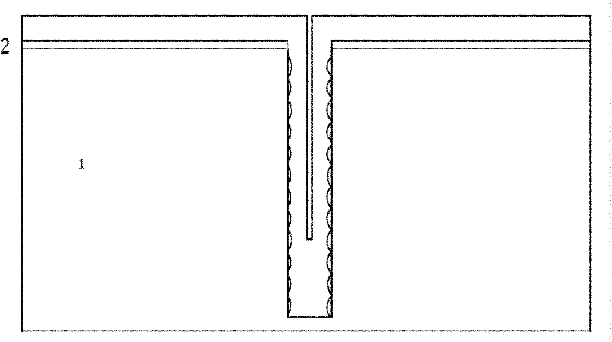
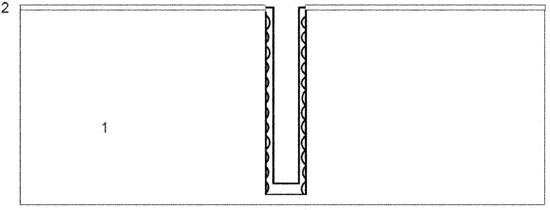
[0030] In a preferred embodiment of the present invention, a method for eliminating the influence of the scallop shape of the side wall of the TSV via hole on the subsequent process and forming an insulating oxide film with good conformal coverage is provided, including: providing a hard A semiconductor substrate with a mask pattern, the hard mask pattern corresponds to a through hole; using the hard mask pattern as a mask, Bosch etching (Bosch etch) is used to etch the semiconductor substrate to form a through hole ; Using a high aspect ratio process (High Aspect Ratio Process, HARP) to partially fill the TSV; using a one-step high-temperature annealing process to heat treat the silicon wafer; use SiCoNi to modify the morphology of the partially...


PUM


Abstract

The invention relates to a through hole processing method which comprises the following steps of: providing a masking film; etching a substrate according to the masking film to form a through hole; partially filling the through hole so as to form an insulated oxidization layer with fixed-shape coverage on the lateral wall of the through hole; and removing the masking film. The through hole processing method provided by the invention can eliminate the influence of a scallop appearance of the lateral wall of a silicon through-hole generated through a Bosh etching process on a follow-up process, and an insulated oxide layer thin film with a smooth surface is formed on the lateral wall of the silicon through-hole, therefore, the fixed-shape coverage performance of the insulated oxide layer thin film is improved, the follow-up silicon through-hole filling difficulty is reduced, and the reliability of device failure is finally reduced.

Description

technical field [0001] The invention relates to the field of semiconductor manufacturing and packaging, in particular to a through-hole processing method in the semiconductor manufacturing process, especially a through-silicon hole processing method. Background technique [0002] As the integration level of integrated circuits continues to increase, semiconductor technology continues to develop rapidly. At present, the development of semiconductor technology follows the road of Moore's law of miniaturization and has developed to 22nm, which has begun to approach its physical limit. At this time, the introduction of other related new technologies can promote the further development of integrated circuits. Among them, Through Silicon Via (TSV) technology is a rare technology that is developing rapidly and will widely affect the technical field of consumer and industrial electronic products. The 3-D IC integration it brings is constantly increasing. Promote the development of...

Claims


Application Information

Patent Timeline
Patent Type & Authority Applications(China)
IPC IPC(8): H01L21/768
Inventor 赵宇航周军
Owner SHANGHAI INTEGRATED CIRCUIT RES & DEV CENT
Why Eureka
Try Eureka