Multi-chipset high-power LED encapsulation structure

An LED packaging, high-power technology, applied in electrical components, electric solid-state devices, circuits, etc., can solve the problem of heat dissipation of high-power LED lighting modules, and achieve excellent heat dissipation, reduced thermal resistance, and reduced costs.

Inactive Publication Date: 2011-07-20
HARBIN INST OF TECH
View PDF4 Cites 12 Cited by
  • Summary
  • Abstract
  • Description
  • Claims
  • Application Information

AI Technical Summary

Problems solved by technology

[0003] The purpose of the present invention is to provide a multi-chipset high-power LED packaging structure in order to solve the heat dissipation problem of the multi-chipset high-power LED lighting module

Method used


Image

  • Multi-chipset high-power LED encapsulation structure
  • Multi-chipset high-power LED encapsulation structure
  • Multi-chipset high-power LED encapsulation structure

Examples


specific Embodiment approach 1

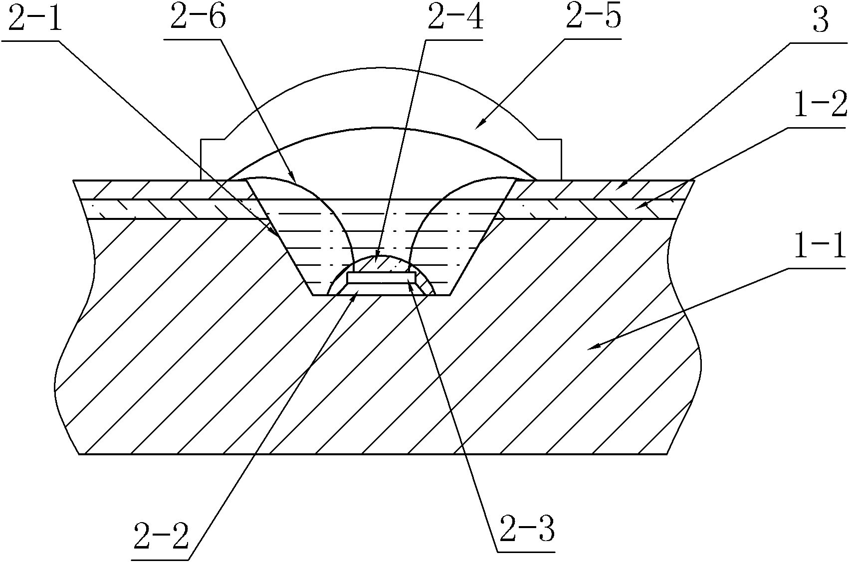
[0021] Specific implementation mode one: the following combination Figure 1 to Figure 3 Describe this embodiment, this embodiment is made up of substrate, a plurality of encapsulating units and circuit wire 3,

[0022] A plurality of packaging units are evenly distributed on the front of the substrate, and circuit wires 3 are printed on the front of the substrate.

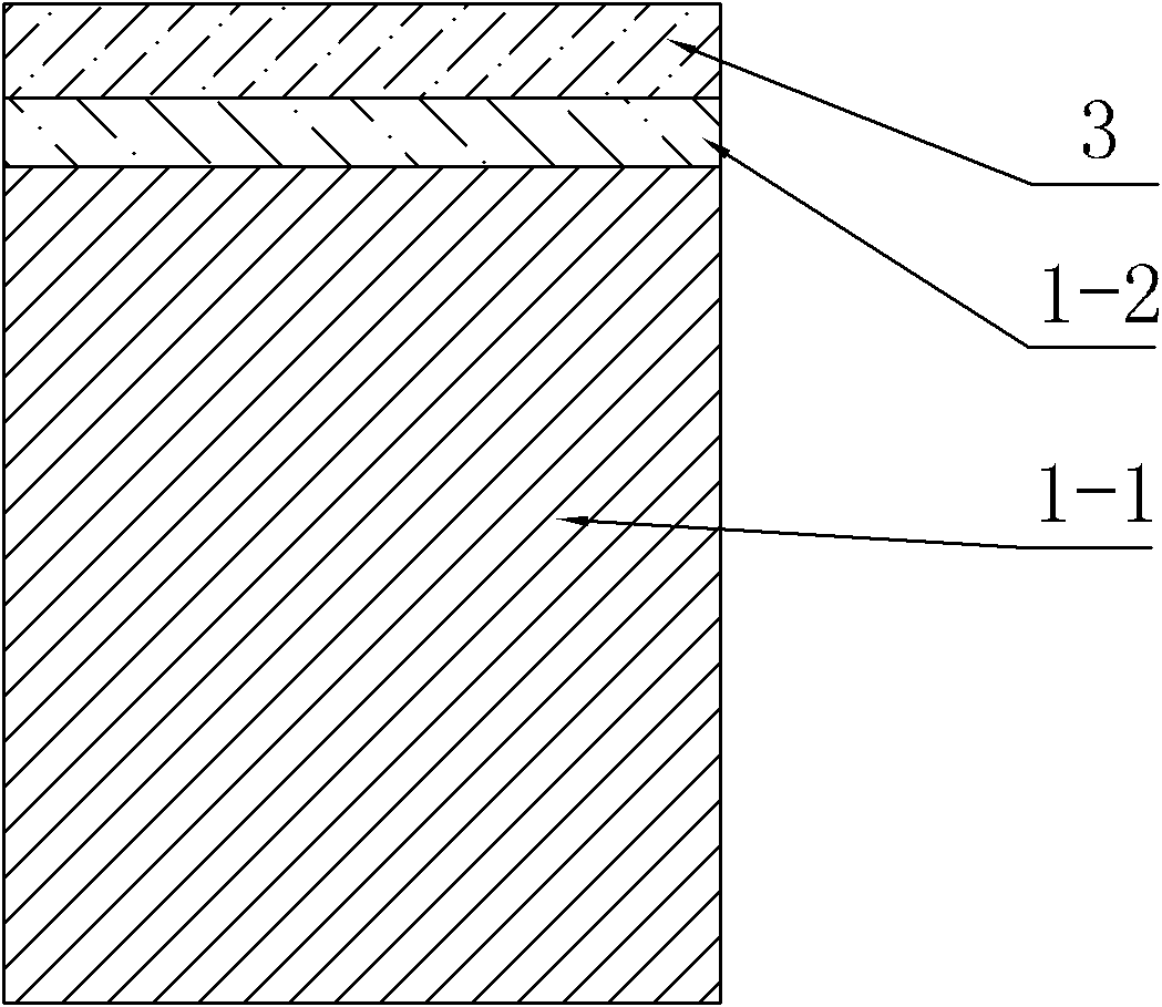
[0023] The substrate is composed of a lower copper heat dissipation substrate 1-1 and an upper insulating layer 1-2,

[0024] Each packaging unit is composed of a reflective cup 2-1, a bonding layer 2-2, an LED chip 2-3, a fluorescent powder 2-4, a silicone lens 2-5 and a gold wire 2-6 for ball bonding,

[0025] The reflective cup 2-1 is opened on the front of the substrate, and the center of the cup bottom of the reflective cup 2-1 is eutectically bonded to the LED chip 2-3, and the upper surface of the LED chip 2-3 is coated with phosphor powder 2-4. The reflective cup 2-1 is filled with silica gel to fix the ...

specific Embodiment approach 2

[0028] Specific implementation mode two: the following combination Figure 2 to Figure 4 Describe this embodiment, this embodiment is made up of substrate, a plurality of encapsulating units and circuit wire 3,

[0029] A plurality of packaging units are evenly distributed on the front of the substrate, and circuit wires 3 are fixed on the front of the substrate.

[0030] The substrate is composed of a lower copper heat dissipation substrate 1-1 and an upper insulating layer 1-2,

[0031] Each packaging unit is composed of a reflective cup 2-1, a bonding layer 2-2, an LED chip 2-3, a fluorescent powder 2-4, a silicone lens 2-5 and a gold wire 2-6 for ball bonding,

[0032] The reflective cup 2-1 is opened on the front of the substrate, and the center of the cup bottom of the reflective cup 2-1 is eutectically bonded to the LED chip 2-3, and the upper surface of the LED chip 2-3 is coated with phosphor powder 2-4 to reflect light. The cup 2-1 is filled with silica gel, and th...

specific Embodiment approach 3

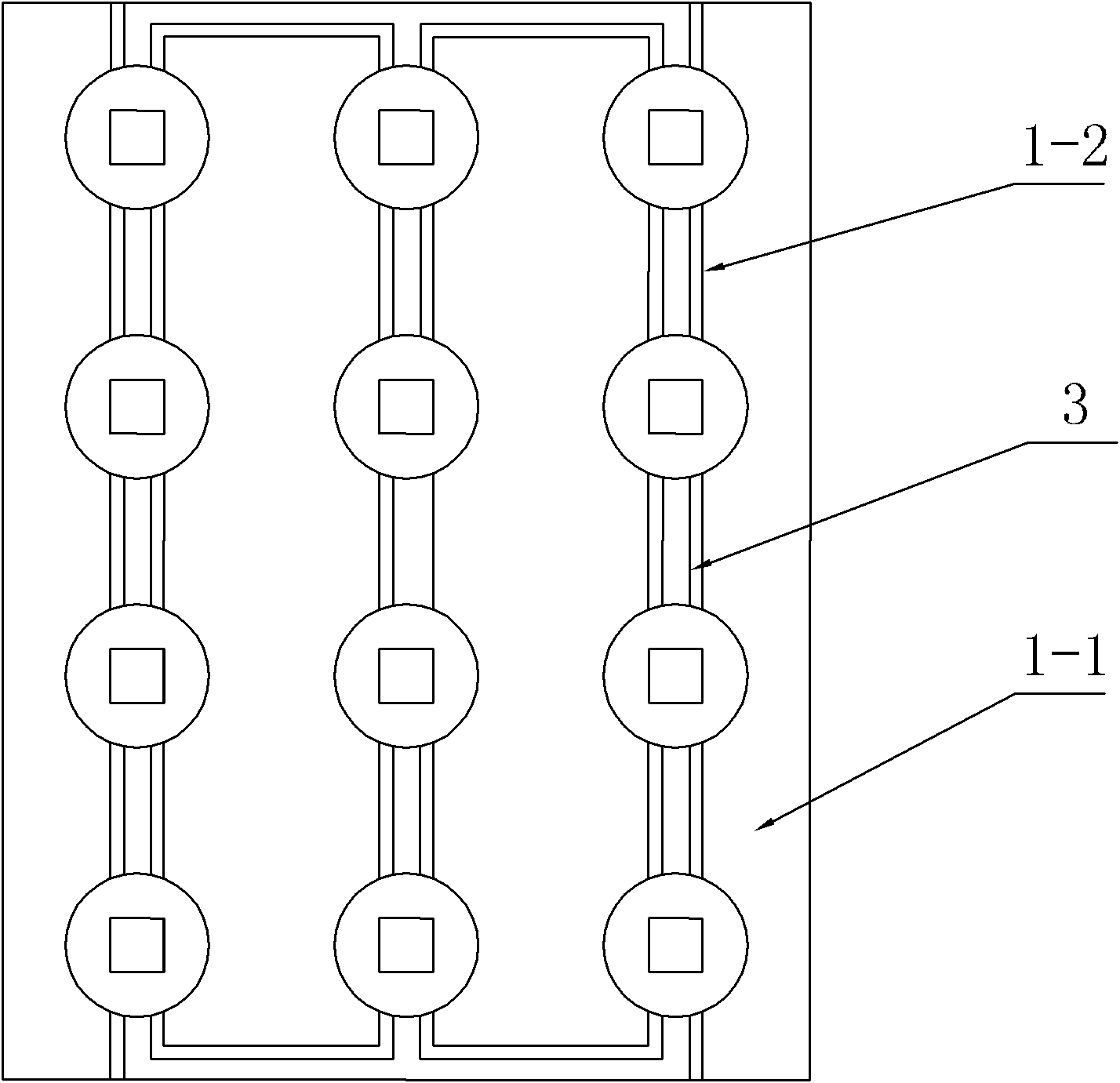
[0035] Specific implementation mode three: the following combination figure 2 This embodiment is described. This embodiment is a further description of Embodiment 1 or 2. The plurality of packaging units are arranged in a matrix on the substrate, and the LED chips 2-3 of all the packaging units in the same row are connected in series to form an LED. groups, multiple LED groups are connected in parallel. Other compositions and connections are the same as those in the first or second embodiment.

[0036] In the matrix arrangement structure of the packaging units described in this embodiment, the distance between them can be controlled by the principle of optical optimization, so as to ensure that the light emitted by the plurality of LED chips 2-3 is uniform.

[0037] figure 2 As shown, the position of each reflector 2-1 is determined according to certain rules, and each reflector 2-1 is packaged with a high-power LED chip 2-3, and each row of four LED chips 2-3 passes throu...


PUM


Abstract

The invention relates to a multi-chipset high-power LED encapsulation structure, belonging to the technical field of LED encapsulation and solving the problem on heat radiation of the multi-chipset high-power LED illumination modules. The multi-chipset high-power LED encapsulation structure comprises a substrate, a plurality of encapsulation units and a circuit lead, wherein the encapsulation units are uniformly distributed on the front side of the substrate; the circuit lead is printed on the front side of the substrate; and the substrate comprises a copper heat-radiating substrate on the lower layer and an insulation layer on the upper layer. Each encapsulation unit comprises a reflecting cup, a bonding layer, an LED chip, fluorescent powder, a silica gel lens and gold wires used for bonding wire balls, wherein the reflecting cup is arranged on the front side of the substrate; the LED chip is bonded on the center of the bottom of the reflecting cup in an eutectic way; the fluorescent powder is coated on the upper surface of the LED chip; silica gel is injected in the reflecting cup for fixing the LED chip; the silica gel lens is fix on the outer side of the mouth of the reflecting cup; and the anode and the cathode of the LED chip are respectively connected with the circuit lead on the front side of the substrate through the gold wires for bonding the wire balls. The invention relates to an encapsulation structure of the LED chips.

Description

technical field [0001] The invention relates to a multi-chip group high-power LED packaging structure, which belongs to the technical field of LED packaging. Background technique [0002] With the continuous progress of the national semiconductor lighting project and the constant call for energy conservation and emission reduction and low-carbon economy, LED lighting has received more and more attention. Compared with traditional incandescent lamps, under the same brightness, LED consumes only one-eighth of the electric energy of incandescent lamps. The application of LED lighting technology will greatly save energy, reduce carbon dioxide emissions, and protect the global environment. High-power LEDs have good application prospects due to their advantages of long life, high luminous efficiency, and energy saving. The greater the power of the LED chip, the more heat it will generate during work, which will lead to a continuous rise in the operating temperature of the chip, ...

Claims


Application Information

Patent Timeline
Patent Type & Authority Applications(China)
IPC IPC(8): H01L25/075H01L33/48H01L33/62H01L33/64H01L33/60H01L33/54
CPCH01L2224/48091H01L2224/73265H01L2224/45144
Inventor 王春青杭春进
Owner HARBIN INST OF TECH
Why Eureka
Try Eureka