Multiple-chip array type chip-on-board (COB) inversely-installed eutectic packaging structure and method

A packaging structure and array technology, applied in electrical components, electrical solid devices, circuits, etc., can solve the problems of poor contact, chip defect luminous efficiency, poor heat dissipation effect, etc., to improve reliability performance, excellent heat dissipation effect, The effect of reducing the bonding temperature

Inactive Publication Date: 2013-10-30
GUANGDONG JINYUAN LIGHTING TECH
View PDF4 Cites 2 Cited by
  • Summary
  • Abstract
  • Description
  • Claims
  • Application Information

AI Technical Summary

Problems solved by technology

There are certain defects in the LED chip package of the existing similar product structure, which include: ①The direct contact between the heating surface and the heat dissipation substrate is not good, the heat generated is not conducive to dissipating through the conduction path, resulting in poor heat diss

Method used


Image

  • Multiple-chip array type chip-on-board (COB) inversely-installed eutectic packaging structure and method
  • Multiple-chip array type chip-on-board (COB) inversely-installed eutectic packaging structure and method
  • Multiple-chip array type chip-on-board (COB) inversely-installed eutectic packaging structure and method

Examples


Embodiment Construction

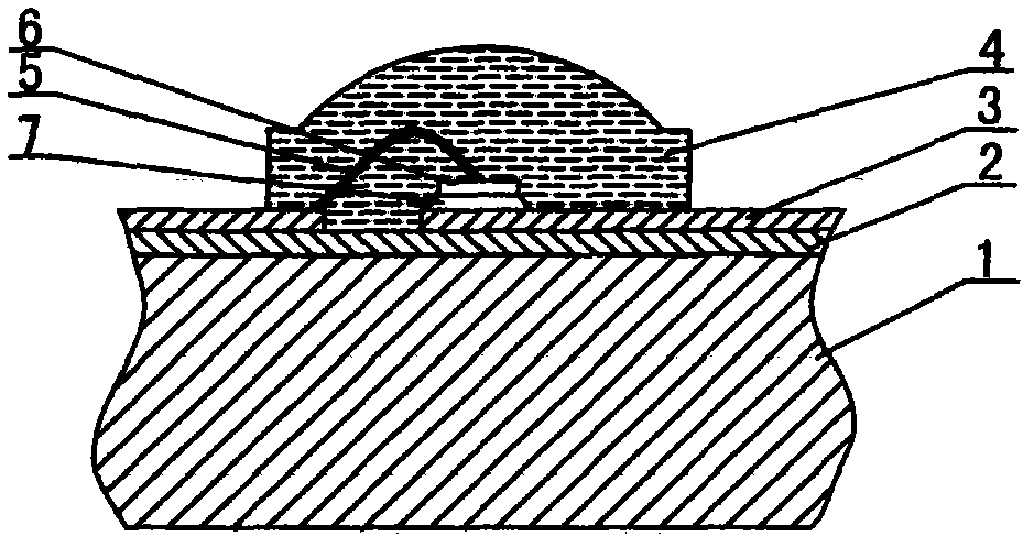
[0020] Such as figure 1 As shown, the multi-chip array COB flip-chip eutectic packaging structure described in the embodiment of the present invention includes a ceramic heat dissipation substrate 1, a phosphor powder and silica gel mixed packaging layer 4, and an LED chip 6. The ceramic heat dissipation substrate 1 is a high thermal conductivity rate, close to the LED chip expansion coefficient of the ALN ceramic substrate and its upper surface is provided with an insulating layer 2, the upper surface of the insulating layer 2 is provided with a circuit wire layer 3, and a plurality of LED chip connection units are installed on the upper side of the ceramic heat dissipation substrate 1; each Each LED chip connection unit is composed of a bonding layer 7, an LED chip 6, and a gold wire 5 for thermosonic bonding, wherein the LED chip 6 is set as a strip-shaped or other-shaped chip whose positive and negative electrodes have different faces and the substrate is transparent. And ...


PUM


Abstract

The invention relates to a multiple-chip array type chip-on-board (COB) inversely-installed eutectic packaging structure and method. The multiple-chip array type COB inversely-installed eutectic packaging structure comprises a ceramic heat-radiating substrate, a fluorescent powder and silica gel mixed packaging layer and light-emitting diode (LED) chips, wherein an insulating layer is arranged on the upper surface of the ceramic heat-radiating substrate, a circuit conductor layer is arranged above the insulating layer, and multiple LED chip connecting units are installed on the upper side of the ceramic heat-radiating substrate. Each LED chip connecting unit consists of a bonding layer, an LED chip and a gold wire shared by thermo-sonic keys, wherein the positive pole ends of the chips are in eutectic bonding with the bonding layers and connected with the circuit conductor layer, and the negative pole ends of the LED chips are connected with one end of the circuit conductor layer on the front side of the substrate through the gold wires. The multiple-chip array type COB inversely-installed eutectic packaging structure and method has the advantages of being excellent in heat-radiating effect and capable of avoiding the problems including chip defects or reduced luminous efficiency and the like caused by the different expansion degree of the chip and the substrate with heat, facilitating wire arrangement, reducing bonding temperature, improving the reliability performance and solving the problems of false welding and unsoldering of wires.

Description

technical field [0001] The invention relates to LED packaging technology, in particular to a multi-chip array COB flip-chip eutectic packaging structure and packaging method. Background technique [0002] LED light-emitting diode packaging refers to the packaging of light-emitting chips, which is quite different from integrated circuit packaging; its packaging is not only required to protect the wick, but also to be able to transmit light. COB packaging is chip On board, which is to adhere the bare chip to the interconnection substrate with conductive or non-conductive adhesive, and then perform wire bonding to realize its electrical connection. There are certain defects in the LED chip package of the existing similar product structure, which include: ①The direct contact between the heating surface and the heat dissipation substrate is not good, the heat generated is not conducive to dissipating through the conduction path, resulting in poor heat dissipation effect; ②When W...

Claims


Application Information

Patent Timeline
IPC IPC(8): H01L25/075H01L33/48H01L33/64H01L33/62
CPCH01L2224/45144H01L2224/48091H01L2224/73265
Inventor 李立群
Owner GUANGDONG JINYUAN LIGHTING TECH
Why Eureka
Try Eureka