LED (light-emitting diode) lamp and manufacturing method thereof

A technology of LED lamps and manufacturing methods, which are applied to lighting devices, cooling/heating devices of lighting devices, light sources, etc., can solve problems such as poor heat dissipation of LED lamps, and achieve good electrical insulation performance, reduced heat dissipation paths, and excellent heat dissipation effects. Effect

Inactive Publication Date: 2012-07-11
SHANGHAI GRANDAR LIGHT ART & TECH
View PDF9 Cites 1 Cited by
  • Summary
  • Abstract
  • Description
  • Claims
  • Application Information

AI Technical Summary

Problems solved by technology

[0005] The technical problem to be solved by the present invention is to provide a direct mounting LED lamp and its manufacturing method in order to overcome the defect of poor heat dissipation of the prior art LED lamp

Method used


Image

  • LED (light-emitting diode) lamp and manufacturing method thereof
  • LED (light-emitting diode) lamp and manufacturing method thereof
  • LED (light-emitting diode) lamp and manufacturing method thereof

Examples


Embodiment 1

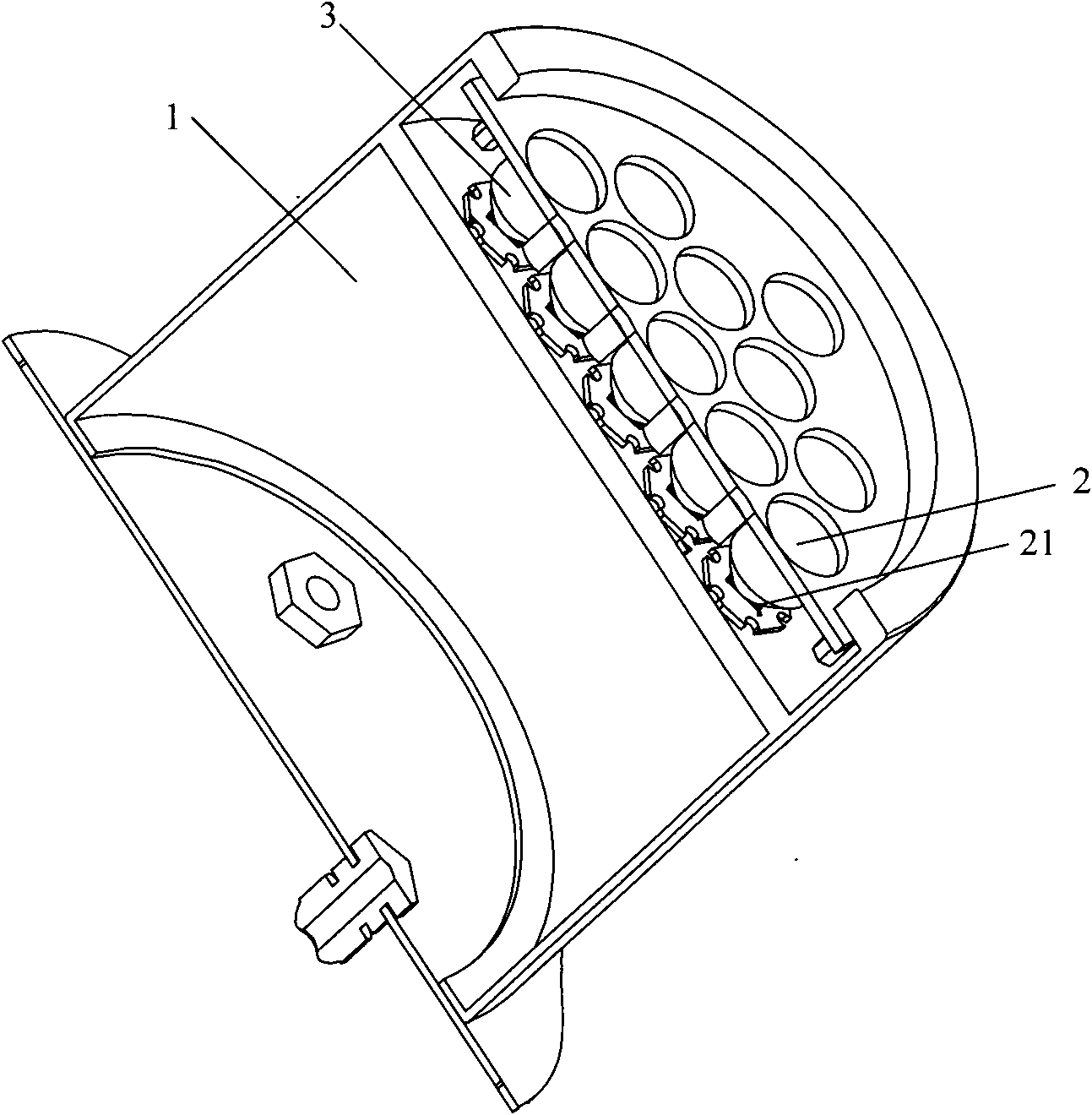
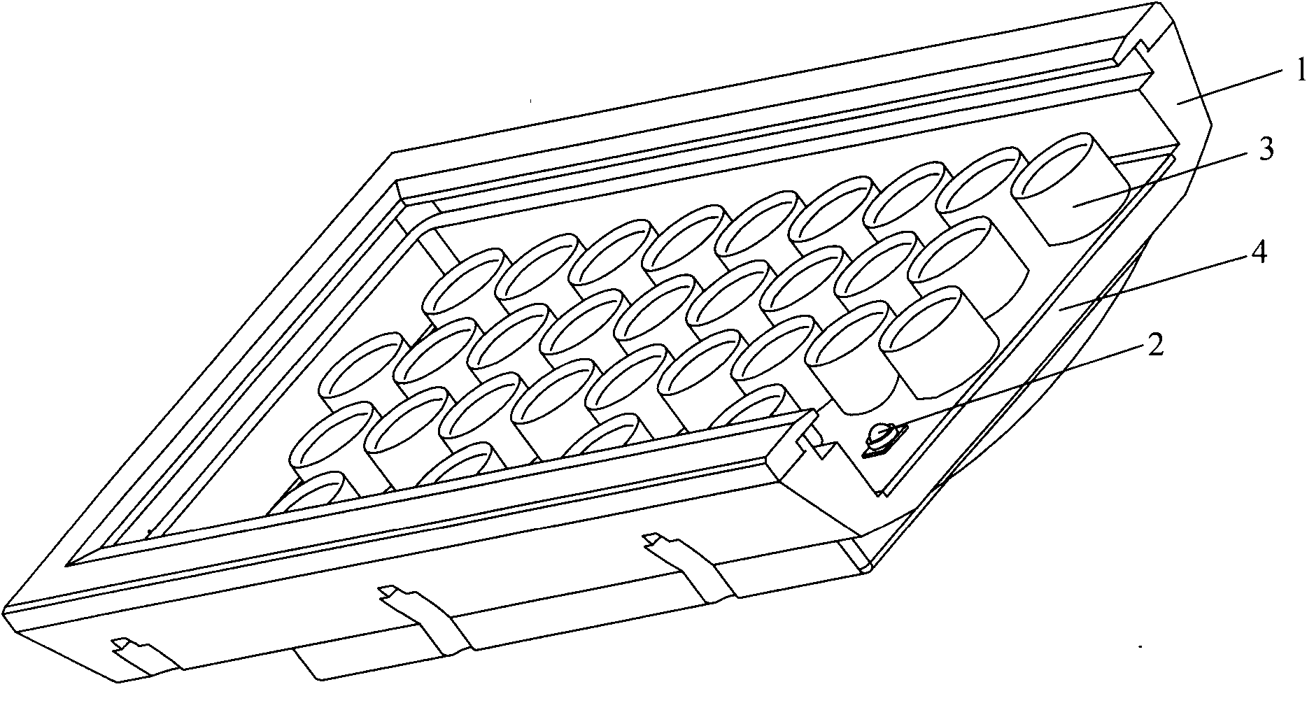
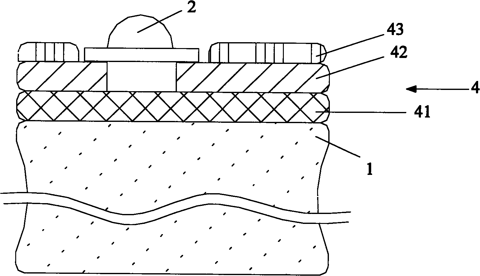
[0048] refer to figure 2 and image 3 , The LED lamp includes a mounting lamp housing 1, an LED 2, and a mounting composite layer 4. The mounting composite layer 4 includes a base insulating layer 41 and a conductive circuit layer 42 in sequence from bottom to top. The chip 21 of the LED2 is mounted on the mounting surface of the conductive circuit layer.

[0049] The insulating base layer 41 plays an insulating role and prevents the circuit short circuit from being in direct contact between the conductive circuit layer 42 and the mounting lamp housing 1 .

[0050] The conductive circuit layer 42 is provided with a mounting surface and a non-mounting surface, and is used for arranging the chips 21 connected to the LED 2 , which helps to ensure stable circuit contact and orderly arrangement.

[0051] Further, an insulating layer 43 is laid on the non-mounting surface of the conductive circuit layer 42 . The insulating layer 43 is located around the LED 2, which can prevent...

Embodiment 2

[0056] This embodiment is basically the same as the first embodiment, the difference being that: a silk screen layer 44 is laid on the insulating layer 43 . The silk screen layer 44 can be used for printing information identifying LED lamps, and serves as a protective insulating layer to further ensure insulating performance. Wherein, the process of silk screen printing is a prior art in this field, and will not be repeated here.

[0057] To sum up, the present invention can reduce the thermal resistance to the minimum by directly mounting the LED on the mounted lamp housing, and effectively export the internal heat, thereby achieving an excellent heat dissipation effect.

[0058] In addition, the present invention also provides a method for manufacturing an LED lamp, which includes the following steps:

[0059] Step 100, perform pretreatment of blanking, pickling, cleaning and drying on the mounted lamp housing.

[0060] Step 101, laying a mounting composite layer on the su...


PUM


Abstract

The invention discloses an LED (light-emitting diode) lamp. The LED lamp comprises an attached lamp shell and an LED, wherein an attached composite layer is laid on the attached lamp shell, and comprises a substrate insulating layer and a conducting wire layer which are arranged in sequence from bottom to top; and the LED or an electronic element are attached on the attached surface of the conducting wire layer. The LED lamp has the advantages that the shell of the LED lamp is directly used as the attached lamp shell of the LED, the radiating way is reduced to have fewest links, and the influences of various heat resistances are avoided, so that the radiating performance is greatly improved, the structure form is simplified and the assembling cost and the product-manufacturing cost are saved.

Description

technical field [0001] The invention relates to the field of lamp lighting, in particular to an LED lamp directly mounted with LEDs and a manufacturing method of the lamp. Background technique [0002] LED lamps are mainly used for daily lighting. They have many advantages such as high luminous efficiency, power saving and long life, so their applications are becoming more and more extensive. Usually, one LED lamp integrates multiple power LEDs, so the heat dissipation of the LED lamp becomes an important factor affecting its use status and lifespan. [0003] At present, heat dissipation aluminum substrate technology is used in LED lamps. like figure 1 As shown, the chip of the LED is connected to the aluminum substrate. When powered on, the LED transfers heat to the aluminum substrate, and then to the lamp housing through the heat dissipation channel. The heat dissipation aluminum substrate is a medium that provides heat conduction, which can increase the bottom area of...

Claims


Application Information

Patent Timeline
Patent Type & Authority Applications(China)
IPC IPC(8): F21S2/00F21V19/00F21V29/00F21Y101/02F21K9/235F21V29/503F21V29/507F21Y115/10
Inventor 汪刚侯彦丽温源
Owner SHANGHAI GRANDAR LIGHT ART & TECH
Why Eureka
Try Eureka