Storage element and storage device

A storage element and storage device technology, applied in electrical elements, electric solid state devices, semiconductor devices, etc., can solve the problem of MRAM power consumption and other problems, and achieve the effects of improving resistance value retention performance, large capacity, and increasing times.

Active Publication Date: 2013-07-24
SONY CORP
View PDF1 Cites 0 Cited by
  • Summary
  • Abstract
  • Description
  • Claims
  • Application Information

AI Technical Summary

Problems solved by technology

MRAM has problems with power consumption

Method used


Image

  • Storage element and storage device
  • Storage element and storage device
  • Storage element and storage device

Examples


Embodiment

[0075] Specific examples of the present invention will be described below.

[0076] With respect to the memory cell array 20 and the memory element 10 in the above-mentioned embodiment, different samples were fabricated to study their properties.

[0077]

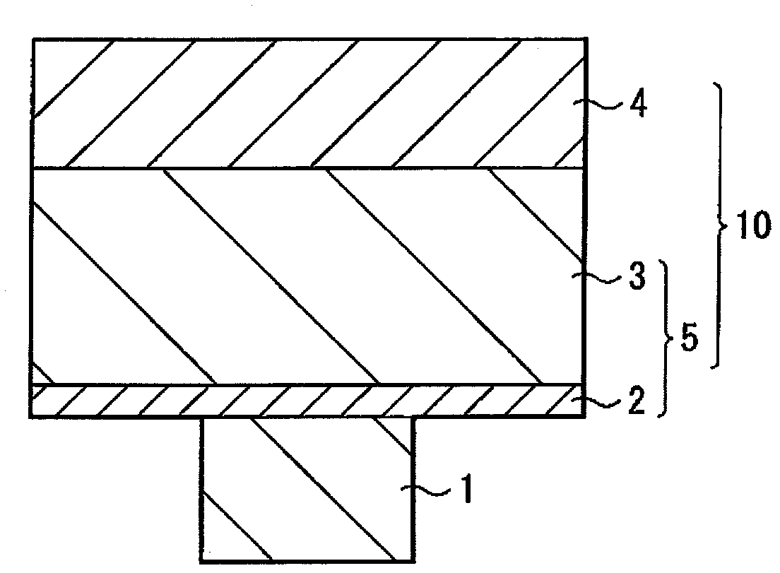
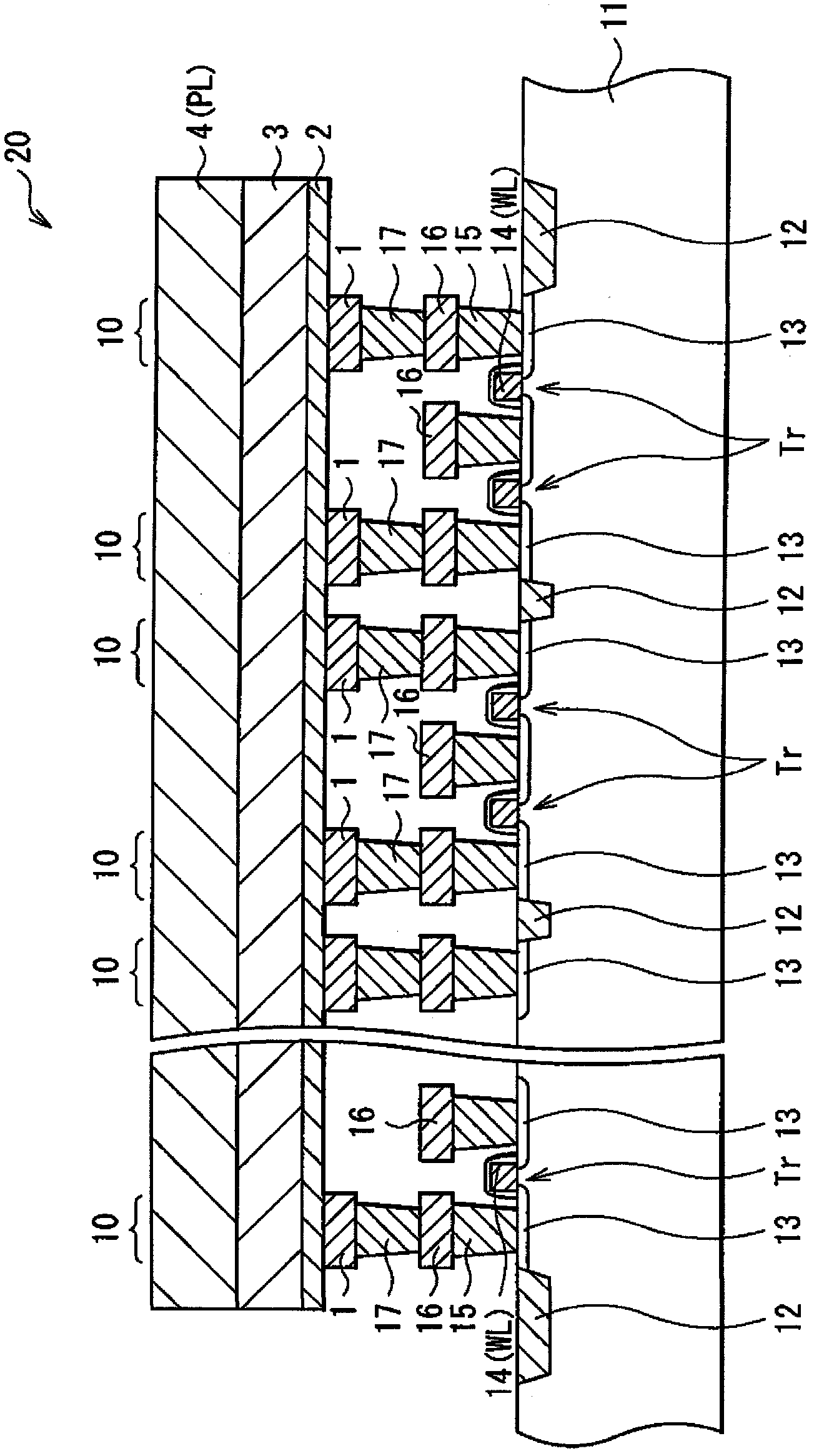
[0078] First, if figure 2 and image 3 As shown, a MOS transistor Tr is formed on a semiconductor substrate 11 . Next, an insulating layer is formed to cover the surface of the semiconductor substrate 11, the insulating layer being formed with via holes. After that, the via hole is filled with an electrode material W (tungsten) by CVD (Chemical Vapor Deposition), and the surface of the resulting via hole is ground by CMP (Chemical Mechanical Polishing). Thereafter, by repeating such processes, the plug layer 15, the metal wire layer 16, and the lower electrode 1 are formed, and then the lower electrode 1 is patterned according to the memory cell. The lower electrode 1 was formed such that its aperture portion had a d...


PUM


Abstract

Provided are a memory element and a memory device. A memory layer is provided with an ion source layer. The ion source layer includes Zr (zirconium), Cu (copper), and Al (aluminum) as a metal element together with an ion conductive material such as S (sulfur), Se (selenium), and Te (tellurium) (chalcogen element). The amount of Al in the ion source layer is 30 to 50 atomic percent. The amount of Zr is preferably 7.5 to 25 atomic percent, and more preferably, the composition ratio of Zr to the chalcogen element in total included in the ion source layer (=Zr (atomic percent) / chalcogen element in total (atomic percent)) falls within a range from 0.2 to 0.74.

Description

technical field [0001] The present invention relates to a memory element capable of storing binary information or multi-valued information including values ​​larger than binary in response to changes in electrical properties in a memory layer including an ion source layer. Background technique [0002] As a nonvolatile memory in which information is not erased even when the power is turned off, types such as flash memory, FeRAM (Ferroelectric Random Access Memory), MRAM (Magnetoresistive Random Access Memory), and the like have previously been proposed. These types of memory are capable of retaining written information for long periods of time without power supply. However, each of these types of memory has its own advantages and disadvantages. In other words, flash memory has a higher packing density but has a disadvantage in terms of operating speed. FeRAM has limitations in terms of miniaturization to build higher packing densities, and also has problems in terms of man...

Claims


Application Information

Patent Timeline
Patent Type & Authority Patents(China)
IPC IPC(8): H01L27/10H01L45/00H01L49/00
CPCH01L45/1233H01L45/1266H01L45/085H01L45/1633H01L45/1625H01L27/2436H01L27/2472H01L45/146H10B63/82H10B63/30H10N70/245H10N70/8416H10N70/826H10N70/028H10N70/8833H10N70/026H10N70/20
Inventor 大场和博水口彻也保田周一郎
Owner SONY CORP
Why Eureka
Try Eureka