
LED (light emitting diode) wafer with evenly distributed current

A technology of uniform current and wafer, applied in circuits, electrical components, semiconductor devices, etc., can solve the problems of low light output efficiency, uneven light emission, small light output area, etc., to achieve uniform current diffusion, prolong service life, and improve light output efficiency. Effect

Inactive Publication Date: 2011-08-03
GUANGDONG TONGFANG ILLUMINATIONS CO LTD
View PDF2 Cites 7 Cited by
  • Summary
  • Abstract
  • Description
  • Claims
  • Application Information

AI Technical Summary

Problems solved by technology

Due to the staggered structure of its electrodes, if there is a slight deviation in the production, the staggered structure is not uniform enough, which will lead to insufficient current diffusion, resulting in uneven light emission, and the light output area is small, there is a limit of total reflection angle, and the light output efficiency is low.

Method used


Image

  • LED (light emitting diode) wafer with evenly distributed current
  • LED (light emitting diode) wafer with evenly distributed current
  • LED (light emitting diode) wafer with evenly distributed current

Examples


Embodiment Construction

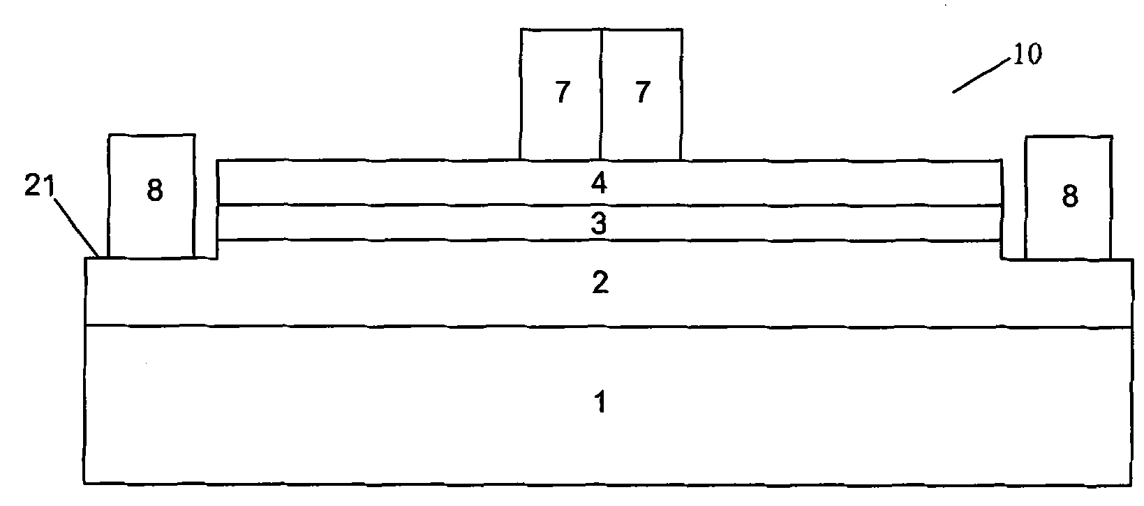
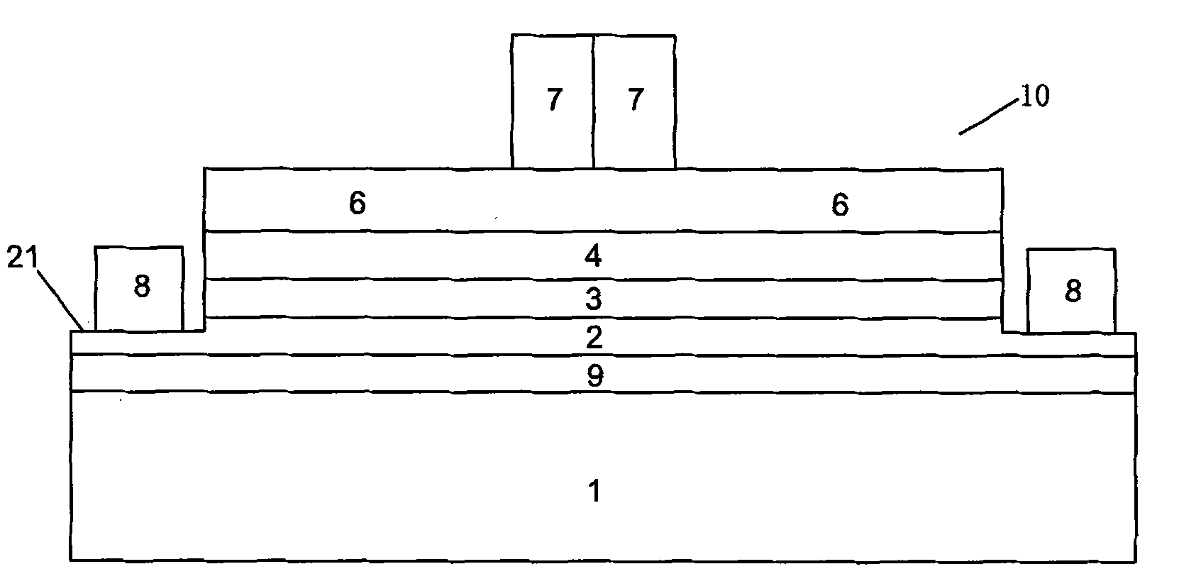
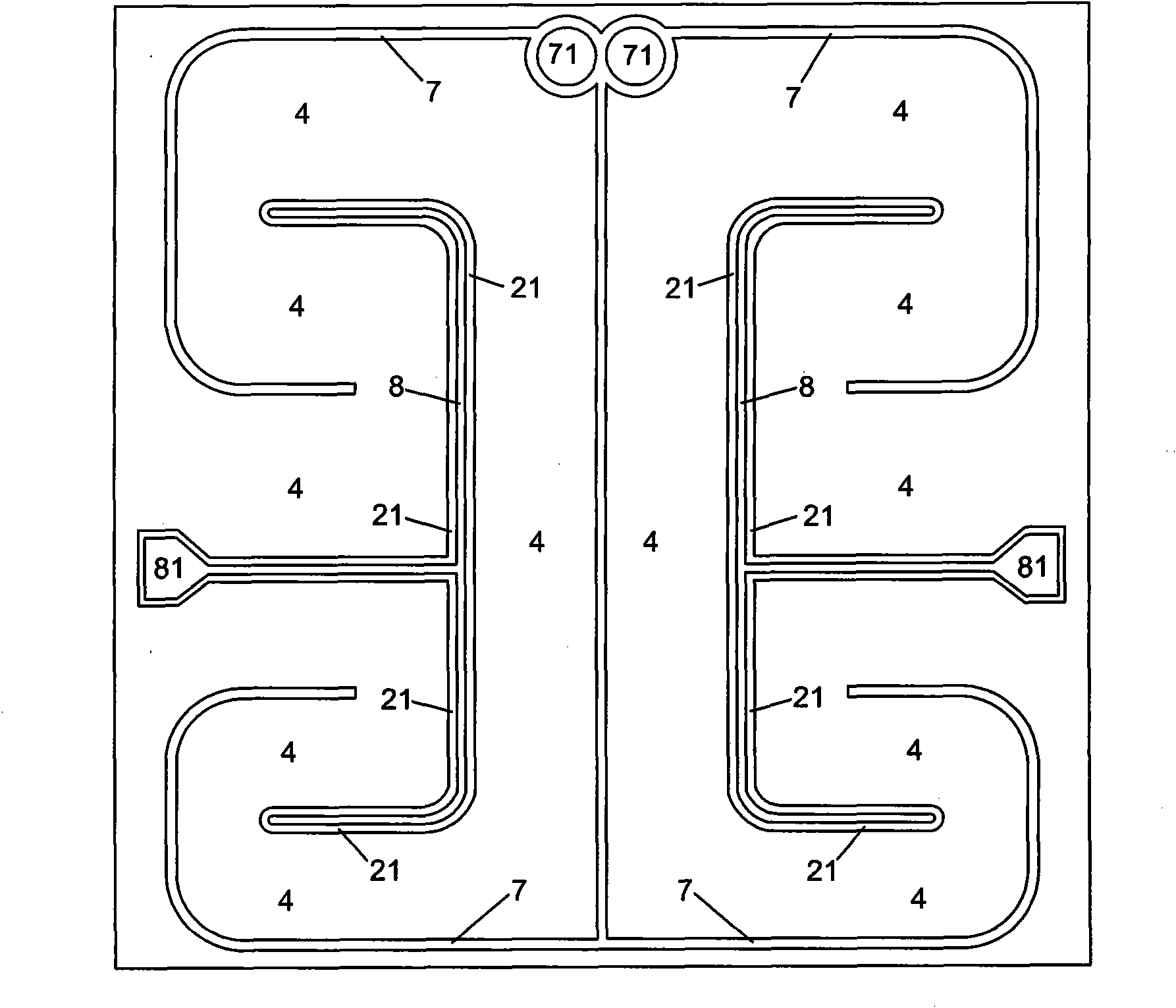
[0017] Refer to attached figure 1 , 2 , 3, and 4, the present invention includes an N-type semiconductor layer 2, a light-emitting layer 3 formed on the N-type semiconductor layer 2; a P-type semiconductor layer 4 formed on the light-emitting layer 3; the surface of the P-type semiconductor layer 4 is provided with A symmetrical "E"-shaped trench 21 connected to the N-type semiconductor layer 2; a negative electrode 8 formed in the symmetrical "E"-shaped trench 21 and a positive electrode 7 formed in the P-type semiconductor layer 4; symmetrical The "E"-shaped groove 21 is covered with the N-type semiconductor layer 2, and the negative electrode 8 is arranged on the symmetrical "E"-shaped groove 21 to form a symmetrical "E"-shaped negative electrode 8, and the positive electrode 7 surrounds the symmetrical Around the "E"-shaped negative electrode 8, a layer of metal is partially vapor-deposited on the positive electrode 7 to form a positive electrode bonding wire area 71 thr...


PUM


Abstract

The invention discloses an LED (light emitting diode) wafer with evenly distributed current, comprising an N-type semiconductor layer, a luminescent layer, a P-type semiconductor layer, negative electrodes and positive electrodes, wherein the luminescent layer is formed on the N-type semiconductor layer; the P-type semiconductor layer is formed on the luminescent layer; the surface of the P-type semiconductor layer is provided with grooves communicated with the N-type semiconductor layer; the negative electrodes are formed on the grooves; and the positive electrodes are formed on the P-type semiconductor layer. The LED wafer is characterized in that the grooves are one pair of symmetrical E-shaped grooves; the symmetrical E-shaped grooves are distributed on the N-type semiconductor layer; the negative electrodes are formed on the grooves to correspondingly form symmetrical E-shaped negative electrodes; and the positive electrodes surround the symmetrical E-shaped negative electrodes. The LED wafer has the advantages of even heat dissipation, high light emission efficiency, long service life and the like.

Description

【Technical field】 [0001] The invention relates to an LED chip, in particular to an LED chip with uniform current distribution. 【Background technique】 [0002] Light-emitting diodes inject current into the active layer located at the P-N junction, and emit light through the radiation recombination of electrons and holes. The wavelength of emitted light is determined by the forbidden band width of the material in the active region. In terms of propagation, one of its main characteristics is that the light emitted by semiconductor light-emitting diodes belongs to spontaneous emission, and the probability of the emitted light propagating to all directions in space is equal. The second main characteristic is that the refractive index of the semiconductor material is relatively large, and the emitted light is emitted from the optically dense medium (such as GaN) into the optically sparse medium (air), so there must be total reflection of light, which limits the light. Output. F...

Claims


Application Information

Patent Timeline
Patent Type & Authority Applications(China)
IPC IPC(8): H01L33/38H01L33/20
Inventor 樊邦扬
Owner GUANGDONG TONGFANG ILLUMINATIONS CO LTD
Learn More