Method for realizing high-efficiency electromagnetic absorption by using transmitted wave/evanescent wave conversion mechanism
A technology for transmitting waves and mechanisms, applied in electrical components, magnetic field/electric field shielding, etc., it can solve the problems that the relationship between parameters and structures cannot be given, the equivalent medium theory is not completely practical, and the numerical simulation optimization is limited, so as to save design. Cost, wide application spectrum, time saving effect
- Summary
- Abstract
- Description
- Claims
- Application Information
AI Technical Summary
Problems solved by technology
Method used
Image

Examples
Embodiment 1
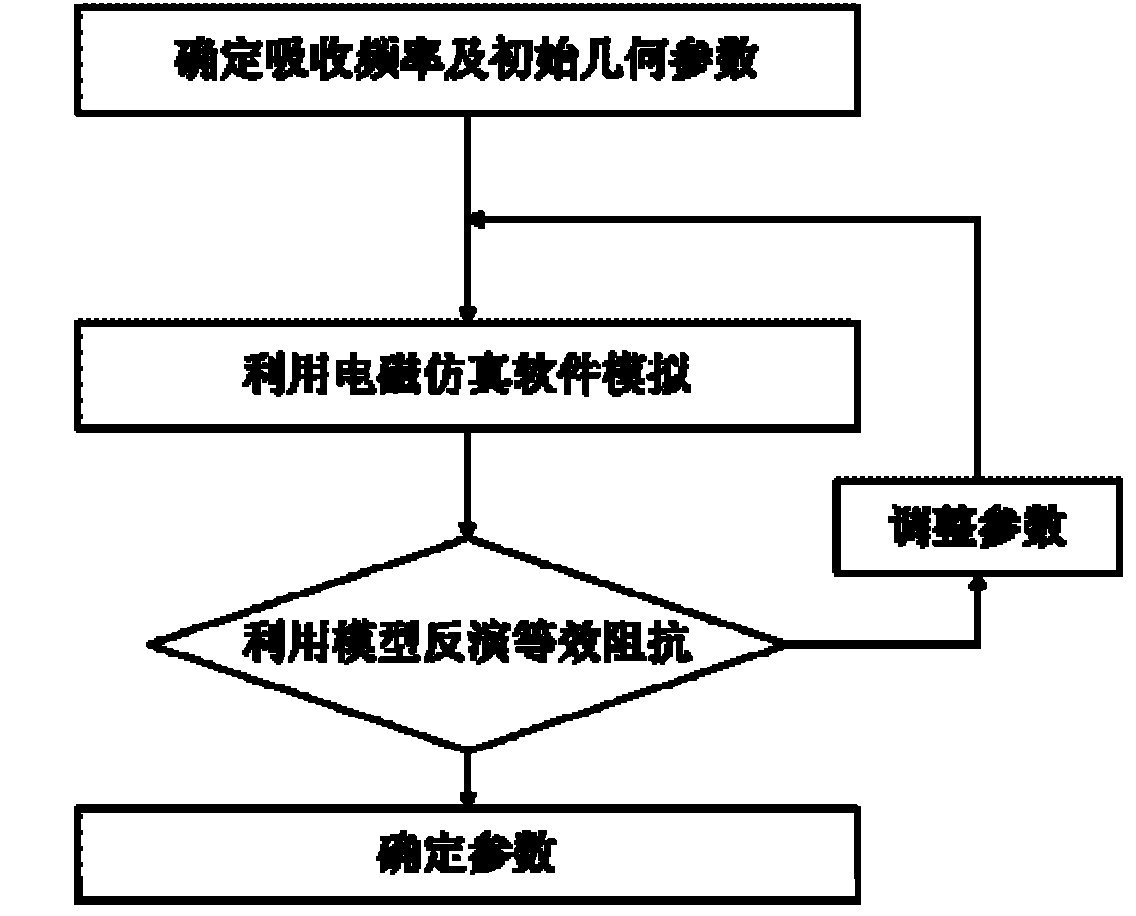
[0034] Such as figure 1 As shown, the specific steps of Embodiment 1 of the present invention are as follows:
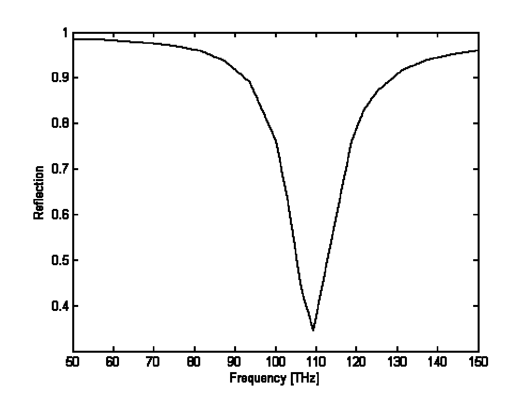
[0035] (1) Determine the absorption frequency as 100THz;
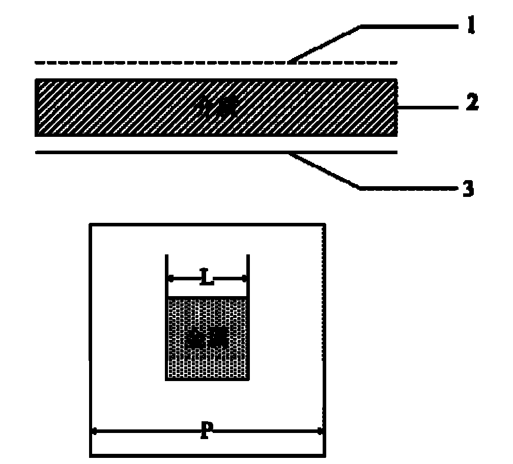
[0036] (2) Choose copper as figure 2 The material of the metal reflective surface indicated by the number 3 in the above figure (side view), the thickness t of copper is much greater than the penetration depth, and t is selected as 100nm.
[0037] (3) Select Al 2 o 3 as figure 2 The material of the medium indicated by the number 2 in the above figure (side view), Al 2 o 3 The dielectric constant is 2.92, and the initial value of thickness d is 60nm, which is much smaller than the wavelength.
[0038] (4) Select the square copper patch as figure 2 The metal structure indicated by the number 1 in the above picture (side view) is made of metallic copper; figure 2 The figure below shows a top view of the structure, in figure 2 In the figure below, the period P is 800nm, the side length L of the cop...
Embodiment 2
[0044] The concrete steps of embodiment 2 of the present invention are as follows:
[0045] (1) Determine the absorption frequency to be 9.5GHz;
[0046] (2) Choose copper as figure 2 The material of the metal indicated by the number 3 in the above picture (side view), the thickness of metal copper is 0.017mm;
[0047] (3) Select FR-4 medium board as figure 2 The material of the medium indicated by the number 2 in the above figure (side view), the dielectric constant of the FR-4 dielectric plate in this frequency band is 4+0.1i, and the initial value of the thickness d is 0.5mm;
[0048] (4) Select the square copper patch as figure 2 The metal structure indicated by the number 1 in the above picture (side view) is made of metallic copper; figure 2The figure below shows a top view of the structure, in figure 2 In the figure below, the period P is 10mm; the side length L of the copper patch is 7mm, and the thickness t is 0.017mm.
[0049] (5) adopt the same steps as i...
PUM
| Property | Measurement | Unit |
|---|---|---|
| Thickness | aaaaa | aaaaa |
| Thickness | aaaaa | aaaaa |
| Dielectric constant | aaaaa | aaaaa |
Abstract
Description
Claims
Application Information
 - R&D
- Intellectual Property
- Life Sciences
- Materials
- Tech Scout
- Unparalleled Data Quality
- Higher Quality Content
- 60% Fewer Hallucinations
Browse by: Latest US Patents, China's latest patents, Technical Efficacy Thesaurus, Application Domain, Technology Topic, Popular Technical Reports.
© 2025 PatSnap. All rights reserved.Legal|Privacy policy|Modern Slavery Act Transparency Statement|Sitemap|About US| Contact US: help@patsnap.com