

Electromagnetic wave shielding protective film and manufacturing method thereof
A production method and technology of protective film, applied to chemical instruments and methods, layered products, metal layered products, etc., can solve the problems of difficult discharge, scratches of protective film, easy generation of bubbles, etc., and achieve fast automatic exhaust speed , The production method is simple, the effect of eliminating static electricity
- Summary
- Abstract
- Description
- Claims
- Application Information
AI Technical Summary
Problems solved by technology
Method used
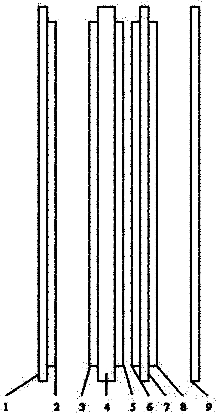
Image

Examples
Embodiment 1
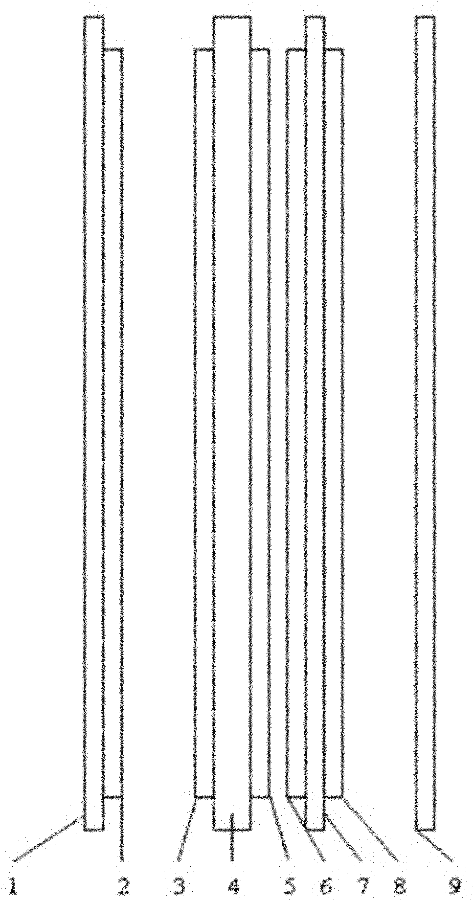
[0038] An electromagnetic wave shielding protective film, comprising: a scratch-resistant layer protective film PET base material (1) with a thickness of 50um, a main film PET base material with a thickness of 150um (4), and a composite PET base material with a thickness of 16um (7) , 50um thick mounting adhesive protective film PET substrate (9), 5um thick protective film adhesive layer (2), 2um thick anti-scratch layer (3), 8um thick composite adhesive layer (5), The metal nanolayer (6) with a thickness of 2um and the installation adhesive layer (8) with a thickness of 25um; It is acrylic resin; the composite adhesive layer (5) is made of polyurethane resin; the metal nano layer (6) is made of nano metal powder.
[0039] The specific steps of the manufacturing method of the above screen protector are as follows:
[0040] (1) Coat a 2 um metal nanolayer (6) on the non-corona surface of the 16um composite PET substrate (7) by high temperature sputtering;
[0041] (2) Coat a ...
Embodiment 2
[0046]An electromagnetic wave shielding protective film, comprising: a scratch-resistant layer protective film PET base material (1) with a thickness of 36 um, a main film PET base material with a thickness of 50 um (4), and a composite PET base material with a thickness of 10 um (7) , 36um thick PET base material for mounting adhesive protective film (9), 10um thick protective film adhesive layer (2), 2um thick anti-scratch layer (3), 4um thick composite adhesive layer (5), The metal nanolayer (6) with a thickness of 2um and the installation adhesive layer (8) with a thickness of 40um; in this embodiment, the protective film adhesive layer (2) and the installation adhesive layer (8) are both made of silicone resin; The scraping layer (3) is made of acrylic resin; the composite adhesive layer (5) is made of polyurethane resin; and the metal nano layer (6) is made of nano metal powder.
[0047] The specific steps of the manufacturing method of the above screen protector are as ...
Embodiment 3
[0053] Embodiment 3. An electromagnetic wave shielding protective film, comprising: a scratch-resistant layer protective film PET substrate (1) with a thickness of 12 um, a main film PET substrate (4) with a thickness of 300 um, and a composite PET substrate with a thickness of 40 um Material (7), mounting adhesive protective film PET substrate with thickness of 12um (9), protective film adhesive layer with thickness of 20um (2), anti-scratch layer with thickness of 8um (3), composite adhesive layer with thickness of 20um (5) The metal nanolayer (6) with a thickness of 3um and the installation adhesive layer (8) with a thickness of 10um; in this embodiment, the protective film adhesive layer (2) and the installation adhesive layer (8) are both made of silicone The anti-scratch layer (3) is made of acrylic resin; the composite adhesive layer (5) is made of polyurethane resin; the metal nano layer (6) is made of nano metal powder.
[0054] The specific steps of the manufacturing...
PUM
| Property | Measurement | Unit |
|---|---|---|
| transmittivity | aaaaa | aaaaa |
| haze | aaaaa | aaaaa |
Abstract
Description
Claims
Application Information