Measuring method and device of laser damaged silicon-based detector

A measurement method and detector technology, applied in the direction of measurement devices, instruments, scientific instruments, etc., can solve problems such as photoelectric sensor damage

Inactive Publication Date: 2011-08-17
CHANGCHUN UNIV OF SCI & TECH
View PDF1 Cites 9 Cited by
  • Summary
  • Abstract
  • Description
  • Claims
  • Application Information

AI Technical Summary

Problems solved by technology

In some special occasions, photoelectric sensors are often used in conjunction with laser light sources, so there is inevitably a problem of laser damage to photoelectric sensors

Method used


Image

  • Measuring method and device of laser damaged silicon-based detector
  • Measuring method and device of laser damaged silicon-based detector
  • Measuring method and device of laser damaged silicon-based detector

Examples


Embodiment

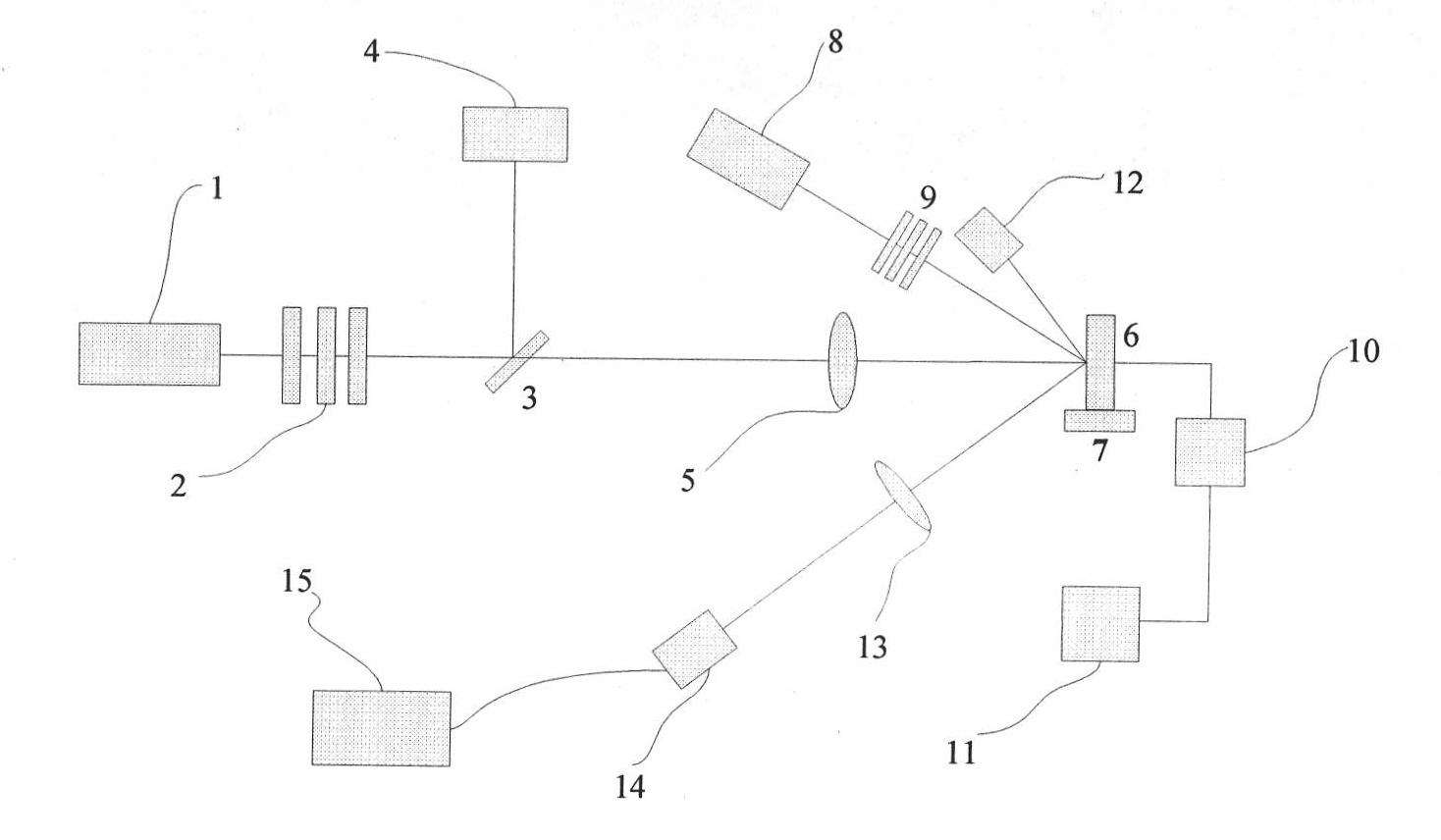
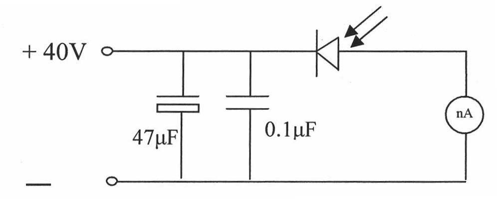
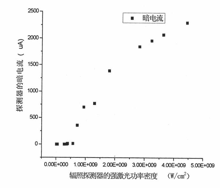
[0020] Implementation example: Taking silicon-based PIN photodetector (model GT102, photosensitive surface diameter 2mm) as an example, study the surface morphology, photocurrent, dark current and Changes in responsivity, and analyze the relationship between detector performance changes and damage levels.

[0021] Such as figure 1 As shown, the output laser power of the He-Ne laser (8) after the attenuator (9) is 56uw, and the silicon-based PIN photodetector works in the linear region at this time. The photocurrent value of the detector measured by the photogalvanometer (11) is 11.76uA, the responsivity of the detector before damage is 0.21uA / uw, and the measured dark current value of the detector is 0.001nA. Adjust the white light diode (12), the imaging lens (13) and the area array CCD (14), so that the detector sample is imaged on the CCD, and stored with a computer. The Nd:YAG laser (1) is irradiated on the surface of the sample (6) through the attenuator (2), the beam s...


PUM

PropertyMeasurementUnit
wavelengthaaaaaaaaaa
diameteraaaaaaaaaa
lengthaaaaaaaaaa

Abstract

A photoelectric detector is the core element of a photoelectric detection system; in special occasions, a photoelectric sensor is usually cooperated with a laser light source, so that damages to the photoelectric sensors by lasers are unavoidable. The invention belongs to the field of photoelectric test, and provides a measuring method and a device of a laser damaged silicon-based detector. The damage degree of a detector by lasers is judged according to the changes of the surface appearance, the light current, the dark current and the responsiveness of the detector before and after strong laser irradiation. Previously, the research to a laser irradiation detector mainly lays particular emphasis on the damage threshold and the damage mechanism, but the changes of the dark current, the light current and the responsiveness during the procedure for quantitatively researching the detector damage are not reported. The method and the device provided by the invention can detect the changes of electric parameters and surface appearance of the detector in the damage procedure in an on-line manner, have the advantages that the detection is overall, accurate and convenient, and are suitable for the damage detection of the silicon-based unit detector and the damage mechanism research of the laser induced detector. And the method and the device provided by the invention can be used in field of laser processing, quality detection of optical elements, development of lasers and the like.

Description

technical field [0001] The invention relates to a measurement method and device for laser damage silicon-based detectors, which can be used for photoelectric testing, and the application fields include the development of detectors, laser processing, scientific research and other fields. Background technique [0002] Photodetectors are the core components of photoelectric detection systems and are widely used in military, industrial, medical and other fields. In some special occasions, photoelectric sensors are often used in conjunction with laser light sources, so there is inevitably a problem of laser damage to photoelectric sensors. After the detector is damaged by strong laser light, its performance will change, manifested as a decrease in responsivity and an increase in dark current. [0003] Scholars at home and abroad have done a lot of theoretical and experimental work on strong laser irradiation detectors, mainly focusing on the damage threshold and damage mechanism...

Claims


Application Information

Patent Timeline
Patent Type & Authority Applications(China)
IPC IPC(8): G01N21/956G01R31/26
Inventor 徐立君蔡红星李昌立谭勇周鸣岐金光勇张喜和
Owner CHANGCHUN UNIV OF SCI & TECH
Why Eureka
Try Eureka