Mode converter having multi-layer structure and optical branching device

A mode conversion, multi-layer structure technology, applied in the directions of light guides, optics, instruments, etc., can solve the problems of low coupling efficiency of optical fibers and waveguides, unstable optical field transmission direction, etc., to reduce size, improve stability, and improve The effect of coupling efficiency

Active Publication Date: 2011-08-17
SHANGHAI SILIGHT TECH
View PDF4 Cites 15 Cited by
  • Summary
  • Abstract
  • Description
  • Claims
  • Application Information

AI Technical Summary

Problems solved by technology

The single-channel mode converter 2 consists of two layers of ridge waveguides, and the coupling efficiency between the fiber and the waveguides is not high
The lateral free propagation region 3 is formed by deep etching, and there is a lateral profile limitation, and the sudden change in thickness makes the light field unstable in the direction of transmission

Method used


Image

  • Mode converter having multi-layer structure and optical branching device
  • Mode converter having multi-layer structure and optical branching device
  • Mode converter having multi-layer structure and optical branching device

Examples


Embodiment Construction

[0021] The present invention will be described in detail below through specific embodiments in conjunction with the drawings:

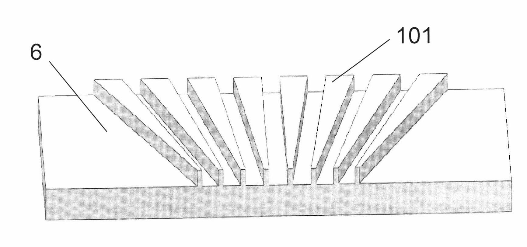
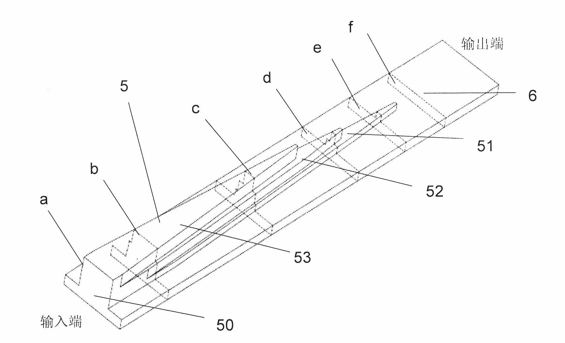
[0022] figure 2 The mode converter in the embodiment of the present invention is given, taking a three-layer ridge waveguide as an example. The ridge waveguide 5 and the slab waveguide 6 are deeply etched on the silicon wafer. The input end 50 of the ridge waveguide 5 is a single ridge waveguide on the slab waveguide 6 formed by deep etching. Three shallow ridge waveguide layers 51, 52, 53. The specific process can be as follows: deep etching is performed on the ridge waveguide 5 to form the ridge waveguide layer 51, then the ridge waveguide layer 51 is etched at a medium depth to form the ridge waveguide layer 52, and finally the ridge waveguide layer 52 is shallowly etched to form the ridge waveguide Layer 53. In this mode converter, the widths of the ridge waveguide layers 51, 52, and 53 gradually narrow from the input end to the output end, and th...


PUM


Abstract

The invention discloses a mode converter having a multi-layer structure and an optical branching device. The mode converter comprises flat waveguides and at least three layers of ridge waveguides which are arranged on the flat waveguide, wherein the width of each layer of ridge waveguides is gradually decreased from an input end to an output end; when the width is decreased to a certain value, the layer of ridge waveguides is cut off, namely one layer of the at least three layers of ridge waveguides is reduced, so that the height of the ridge waveguides is reduced gradually; the input end is farther away from a cut-off position of the ridge waveguides of the optical flat waveguides; and the output end of the mode converter consists of the single-layer flat waveguides and the single-layer ridge waveguides. A transverse free propagation area of the optical branching device consists of the flat waveguides without transverse limitation. Compared with the prior art, a technology provided by the invention has the advantages that: the efficiency of coupling from optical fibres to an optical device can be improved, a one-step etching process is reduced, and the stability of mode transmission in the optical device is improved at the same time.

Description

Technical field [0001] The invention relates to an integrated optoelectronic device, in particular a mode converter and an optical splitter. Background technique [0002] The optical waveguide and planar optical integrated circuit PLC based on silicon SOI on an insulating substrate can help reduce the cost of optical chips and realize multi-functional monolithic integration. However, in the planar optical integrated circuit based on SOI or other high material refractive index contrast, the scattering loss at the branch node is an obstacle to the construction of low-loss devices. [0003] Invention patent 200810092207.0 discloses a SOI optical splitter based on parallel mode converter, see figure 1 . The optical splitter is composed of an incident coupling optical waveguide 1, a single-channel mode converter 2, a lateral free propagation zone 3 and a mode converter 4 connected in sequence. The single-channel mode converter 2 is composed of two layers of ridge waveguides, and the c...

Claims


Application Information

Patent Timeline
Patent Type & Authority Applications(China)
IPC IPC(8): G02B6/14G02B6/122
Inventor 李冰杨晶洪小刚
Owner SHANGHAI SILIGHT TECH
Why Eureka
Try Eureka