Semiconductor device, chip-on-chip mounting structure, method of manufacturing the semiconductor device, and method of forming the chip-on-chip mounting structure

A chip mounting and manufacturing method technology, applied in semiconductor/solid-state device manufacturing, semiconductor devices, semiconductor/solid-state device components, etc., can solve problems such as short circuits

Inactive Publication Date: 2011-08-24
SONY CORP
View PDF4 Cites 13 Cited by
  • Summary
  • Abstract
  • Description
  • Claims
  • Application Information

AI Technical Summary

Problems solved by technology

As a result, electromigration occurs so that Sn atoms move between adjacent solder bump electrodes through small pores in the underfill material and also cause short circuits

Method used


Image

  • Semiconductor device, chip-on-chip mounting structure, method of manufacturing the semiconductor device, and method of forming the chip-on-chip mounting structure
  • Semiconductor device, chip-on-chip mounting structure, method of manufacturing the semiconductor device, and method of forming the chip-on-chip mounting structure
  • Semiconductor device, chip-on-chip mounting structure, method of manufacturing the semiconductor device, and method of forming the chip-on-chip mounting structure

Examples


no. 1 approach

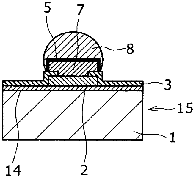
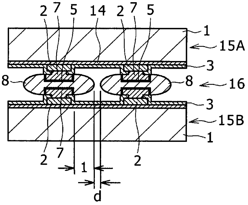
[0052] Figure 1A with 1B The structure of the semiconductor device (semiconductor chip) 15 according to the first embodiment of the present invention is schematically illustrated.

[0053] The semiconductor device 15 is composed of a semiconductor substrate 1 made of Si or the like, a pad electrode 2 made of aluminum, an insulating film 14 (corresponding to the insulating film 64 previously described in the related art), a protective film 3 (corresponding to the previous The protective film 53 ), the copper (Cu) plating layer 5 , the Ni plating layer 7 , the Sn-based solder bump electrode 8 , and the like described in the related art are constituted. Likewise, the under bump metallurgy (UBM) layer is composed of Ni plating layer 7 and Cu plating layer 5 . The size of the solder bump electrode 8, for example, its diameter may be equal to or smaller than 30 μm and its height may be equal to or smaller than 15 μm.

[0054] Such as Figure 1A As shown, it is important for the...

no. 2 approach

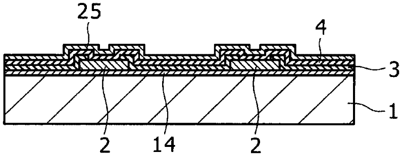
[0073] Figure 3A ~ 3I A semiconductor device according to a second embodiment of the present invention, and steps for manufacturing the semiconductor device of the second embodiment are illustrated respectively.

[0074] First, similar to the reference Figures 4A-4H In the case of the description given, the insulating film 14 , the pad electrode 2 , the protective film 3 , the Ti sputtering layer 4 , the Cu sputtering layer 25 , and the Ni plating layer 7 are sequentially formed on the semiconductor substrate 1 .

[0075] Next, if Figure 3B As shown, the Cu sputtering layer 25 except the portion of the Cu sputtering layer 25 under the Ni plating layer 7 is selectively etched away using the Ni plating layer 7 as an etching mask.

[0076] Next, if Figure 3C As shown, the Ti sputtering layer 4 except for the portion of the Ti sputtering layer 4 under the Ni plating layer 7 is selectively etched away using the Ni plating layer 7 as an etching mask.

[0077] Next, if Figure...


PUM


Abstract

The invention provides a semiconductor device, a chip-on-chip mounting structure, a method of manufacturing the semiconductor device and a method of forming the chip-on-chip mounting structure. The semiconductor device includes: a semiconductor chip having a semiconductor substrate; a pad electrode formed on the semiconductor substrate; a base metal layer formed on said pad electrode; and a bump electrode formed on the base metal layer, in which an exposed surface including a side surface of the base metal layer is covered with the solder bump electrode. As a result, even when the interval between the adjacent solder bump electrodes is reduced, the yield and reliability of the bonding are enhanced.

Description

[0001] Cross References to Related Applications [0002] This application contains subject matter related to and claims priority from Japanese Patent Application JP 2010-026484 filed in the Japan Patent Office on Feb. 9, 2010, the entire content of which is hereby incorporated by reference. technical field [0003] The present invention relates to a semiconductor device suitable for manufacturing electronic devices and a manufacturing method thereof, a chip-on-chip mounting structure using the semiconductor device and a forming method thereof. Background technique [0004] Heretofore, semiconductor devices having solder bump electrodes have been used as key parts of electronic devices such as video equipment such as television receivers, audio equipment, mobile phones, and personal computers. [0005] Figures 4A-4O The steps for producing a semiconductor chip as a semiconductor device 65 are each illustrated. These manufacturing steps described below are disclosed, for exa...

Claims


Application Information

Patent Timeline
Patent Type & Authority Applications(China)
IPC IPC(8): H01L23/00H01L23/488H01L25/00H01L21/603
CPCH01L2224/05562H01L2924/01046H01L2224/13023H01L25/0657H01L2924/0105H01L2224/05155H01L2224/1146H01L2224/05027H01L2924/01019H01L2924/01029H01L2224/11849H01L2224/1147H01L2224/0347H01L24/11H01L2924/014H01L2924/01013H01L2924/3841H01L2924/0103H01L25/50H01L2224/81097H01L2224/05124H01L2924/01047H01L2224/0346H01L24/05H01L24/13H01L2224/05166H01L2224/05647H01L2224/11912H01L2225/06513H01L2924/01005H01L2924/01033H01L2924/01006H01L2224/1181H01L23/3114H01L2924/01078H01L2224/05022H01L2224/131H01L2224/13111H01L2224/0401H01L2924/0002H01L2924/00014H01L2924/01014H01L2224/05552
Inventor 尾崎裕司浅见博
Owner SONY CORP
Why Eureka
Try Eureka