Device and method for detecting rich-Te phase in telluride semiconductor crystal

A semiconductor and telluride technology, which is applied in the field of detection devices, can solve the problems of inability to achieve layered domain focusing imaging, large field of view, and difficult to obtain size.

Active Publication Date: 2012-10-31
IMDETEK
View PDF0 Cites 0 Cited by
  • Summary
  • Abstract
  • Description
  • Claims
  • Application Information

AI Technical Summary

Problems solved by technology

[0004] In order to overcome the shortcomings of the existing devices for detecting Te-rich phases in semiconductor crystals that are difficult to obtain a larger field of view and cannot achieve focused imaging of layered domains in the thickness direction of the crystal, the present invention provides a method for detecting Te-rich phases in telluride semiconductor crystals. phase device

Method used


Image

  • Device and method for detecting rich-Te phase in telluride semiconductor crystal
  • Device and method for detecting rich-Te phase in telluride semiconductor crystal
  • Device and method for detecting rich-Te phase in telluride semiconductor crystal

Examples


Embodiment 1

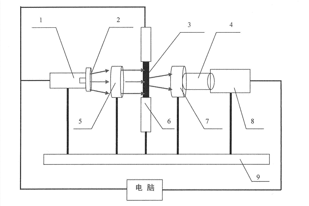
[0028] Embodiment 1 (device embodiment): The device for detecting the Te-rich phase in telluride semiconductor crystals of the present invention includes a light source 1, a lens 2, a lens barrel 4, an optical filter 5, a stage 6, an objective lens 7 and an infrared CCD 8. Among them, the light source 1 uses a halogen tungsten lamp with a spectral range of 360-2000nm as the radiation source for illuminating the crystal 3, and is fixed on one end of the optical vibration isolation platform 9 through a support rod, and the intensity of the light source 1 is controlled by a computer. A lens 2 is placed at the output end of the light source 1, and the focusing degree of light can be adjusted by changing the distance between the lens 2 and the light source 1. A filter 5 is placed behind the lens 2 and fixed on an optical vibration isolation platform 9 with a support rod to obtain monochromatic light for illuminating the sample. The stage 6 is a three-dimensional automatic translati...

Embodiment 2

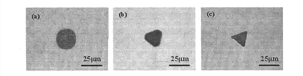
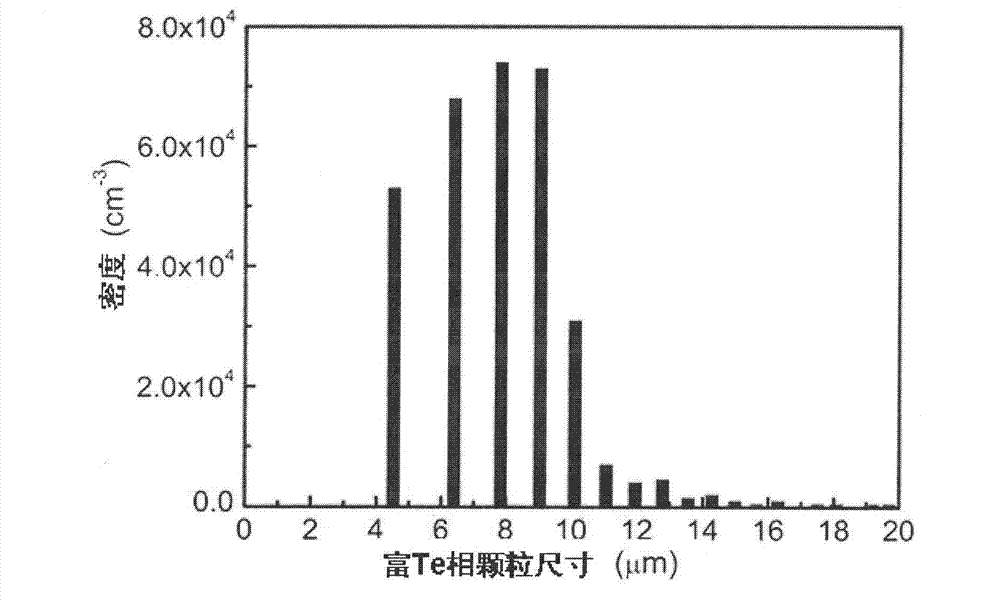
[0030] Example 2: The detection size is 10×10×2mm 3 The size, shape and density of Te-rich phase particles in CdZnTe crystals. Proceed as follows:

[0031] (a) Turn on the power of light source 1 and infrared CCD8, and preheat for 20 minutes, so that the output light intensity is stable, and the imaging noise and chromatic aberration of infrared CCD8 are small. At the same time, select the filter 5 with a wavelength of 980nm.

[0032] (b) Fix the processed CdZnTe crystal 3 on the stage 6, adjust the power output current of the light source 1 to 5.9A, and the luminous flux to be 1450lm, and move the position of the lens 2 horizontally, so that the image gray value collected by the infrared CCD 8 is between 150. The positions of the X, Y and R axes on the stage 6 are adjusted so that the beam line irradiates the CdZnTe crystal 3 to be tested vertically. At the same time, adjust the CdZnTe crystal 3 to be tested, the infrared objective lens 7, and the centers of the infrared C...

Embodiment 3

[0037] Embodiment 3: The detection size is 10×10×2mm 3 The size, shape and density of Te-rich phase particles in CdTe crystals. Proceed as follows:

[0038] (a) Turn on the power of light source 1 and infrared CCD8, and preheat for 20 minutes, so that the output light intensity is stable, and the imaging noise and chromatic aberration of infrared CCD8 are small. At the same time, select the filter 5 with a wavelength of 980nm.

[0039] (b) Fix the processed CdTe crystal 3 on the stage 6, adjust the power output current of the light source 1 to 6.4A, and the luminous flux to 1550lm, and move the position of the lens 2 horizontally so that the gray value of the image collected by the infrared CCD 8 reaches 125. Adjust the positions of the X, Y axes and the rotation R axis in the stage 6 to ensure that the beam line irradiates the CdTe crystal 3 to be tested vertically. At the same time, adjust the center of the CdTe crystal 3 to be tested, the infrared light objective lens 7,...


PUM

PropertyMeasurementUnit
sizeaaaaaaaaaa

Abstract

The invention discloses a device and a method for detecting a rich-Te phase in a telluride semiconductor crystal. By the device and the method, the technical problems that the conventional device for detecting the rich-Te phase in the telluride semiconductor crystal cannot obtain a larger-size visual field and realize focused imaging of a layered domain in the thickness direction of the crystal can be solved. The technical scheme is that: the visual field can be adjusted by changing the magnifying power of a zoom lens barrel; meanwhile, by adoption of a high-precision four-coordinate three-dimensional automatic translational table, the body density of the rich-Te phase can be observed. By the method for detecting the rich-Te phase in the telluride semiconductor crystal by using the detecting device, the focused imaging of the layered domain is realized by adjusting the position in the thickness direction, so the form of the rich-Te phase in the crystal can be observed; and a Labview-based image collection and processing system is used for splicing every collected independent picture into a whole large image at first, counting different gray scale regions of the spliced image and analyzing the distribution of the rich-Te phase in the crystal.

Description

technical field [0001] The invention relates to a detection device, in particular to a device for detecting Te-rich phase in telluride semiconductor crystals. It also relates to a method for detecting the Te-rich phase in the telluride semiconductor crystal by using the detection device. Background technique [0002] refer to Figure 7 , the literature "P.Rudolph, A.Engel, I.Schentke, A.Grochocki, Journal of CrystalGrowth, 1995, 147: 297-304" discloses a device for detecting Te-rich phases in CdTe and CdZnTe crystals, that is, in ordinary optical Modified on the basis of the microscope, the device includes a light source 1 for irradiating samples, a stage 6 for holding a crystal 3, an objective lens 7, a lens barrel 4, an infrared CCD 8, and a support rod 10 and a base 11 for fixing optical components. However, since the stage 6 cannot be accurately positioned in the horizontal direction, the field of view of observation is limited, and the field of view observed is usually...

Claims


Application Information

Patent Timeline
Patent Type & Authority Patents(China)
IPC IPC(8): G01N15/02G01N9/24
Inventor 介万奇徐亚东王涛查钢强何亦辉郭榕榕
Owner IMDETEK
Why Eureka
Try Eureka