Integrated circuit structure and method to stop contact metal from extruding into gate

A gate structure and contact hole technology, applied in the direction of circuits, electrical components, electrical solid devices, etc., to achieve the effect of increasing the pass rate and performance

Active Publication Date: 2011-08-31
TAIWAN SEMICON MFG CO LTD
View PDF5 Cites 5 Cited by
  • Summary
  • Abstract
  • Description
  • Claims
  • Application Information

AI Technical Summary

Problems solved by technology

[0004] However, when it comes to integrating a high-k gate

Method used


Image

  • Integrated circuit structure and method to stop contact metal from extruding into gate
  • Integrated circuit structure and method to stop contact metal from extruding into gate
  • Integrated circuit structure and method to stop contact metal from extruding into gate

Examples


Embodiment Construction

[0071] Hereinafter, each embodiment is described in detail and examples accompanied by accompanying drawings are used as a reference basis of the present invention. In the drawings or descriptions in the specification, the same reference numerals are used for similar or identical parts. And in the drawings, the shapes or thicknesses of the embodiments may be enlarged, and marked for simplicity or convenience. Furthermore, the parts of each element in the drawings will be described separately. It should be noted that the elements not shown or described in the drawings are forms known to those skilled in the art. In addition, the specific embodiment is only A specific method used in the present invention is disclosed, which is not intended to limit the present invention.

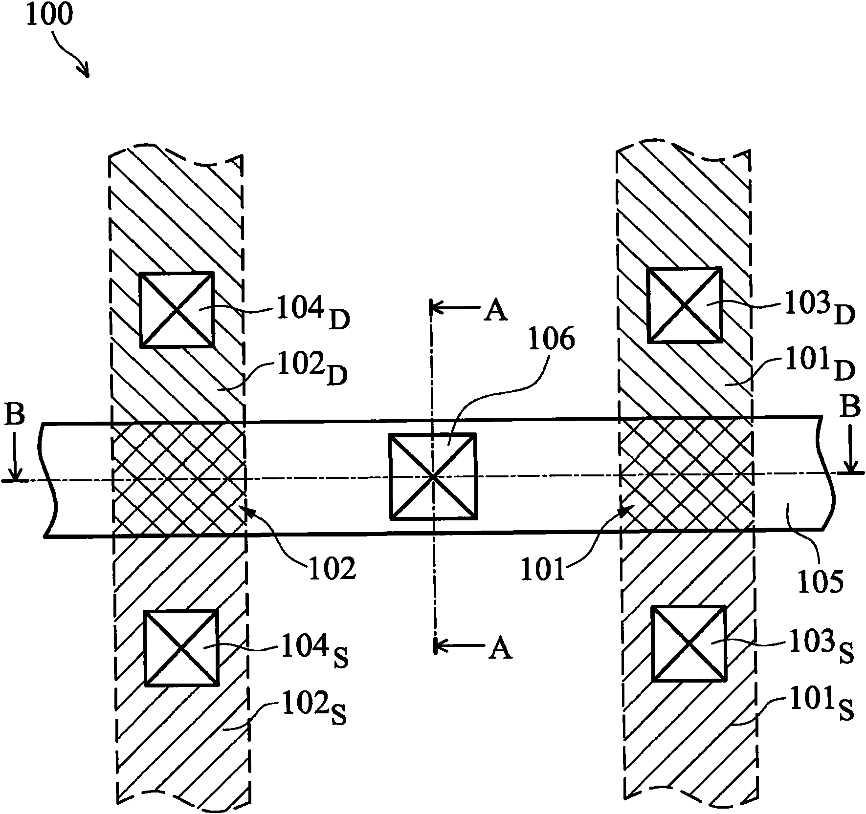
[0072] Figure 1A It is a layout top view of a part of static random access memory (SRAM for short) unit 100 according to an embodiment of the present invention. The SRAM cell 100 includes a pulldown gate 10...


PUM


Abstract

The invention provides an integrated circuit structure and method to methods and structures used to prevent protrusion of contact metal (such as W) horizontally into gate stacks of neighboring devices to affect the work functions of these neighboring devices. A metal gate below a contact plug is defined by a work function layer with good sidewall coverage function and used as a gasket layer of the metal gate, wherein the contact plug is the neighboring device and in common use with (or connected to) the metal gate and the work function layer has good ladder coverage function to prevent the contact metal extruding into the gate stacks of the neighboring devices. Only modification to the mask layout for the photomask(s) used for removing dummy polysilicon is involved. No additional lithographical operation or mask is needed. Therefore, no modification to the manufacturing processes or additional substrate processing steps (or operations) is involved or required. The benefits of using the methods and structures described above may include increased device yield and performance.

Description

technical field [0001] The invention relates to a metal protrusion, in particular to a contact hole metal protruding into a replacement grid. Background technique [0002] The integrated circuit (IC) industry has experienced rapid growth. Technological advances in integrated circuit (IC) materials and design have resulted in each IC generation having smaller and more complex circuits than the previous generation. However, these developments increase the complexity of integrated circuit processes and manufacturing methods, and in order to realize these technological developments, simpler integrated circuit processes and manufacturing methods need to be developed. [0003] During the development of integrated circuits, when the geometric size (meaning the smallest component (or line width) that can be manufactured by a process) shrinks, the functional density (functional density) (meaning the number of interconnections per chip area) usually increases. number of components)....

Claims


Application Information

Patent Timeline
IPC IPC(8): H01L21/283H01L21/336H01L27/105
CPCH01L29/66545H01L29/78H01L21/823842H01L29/4966
Inventor 张立伟朱鸣李季儒锺昇镇游凯翔庄学理
Owner TAIWAN SEMICON MFG CO LTD
Why Eureka
Try Eureka