Thin film transistor with single-gate double-channel structure and manufacturing method thereof

A technology of thin film transistors and manufacturing methods, which is applied in the direction of transistors, semiconductor/solid-state device manufacturing, semiconductor devices, etc., can solve the problems of single function of thin film transistors, and achieve the effect of improving current driving ability

Active Publication Date: 2011-09-14
王磊 +1
View PDF3 Cites 42 Cited by
  • Summary
  • Abstract
  • Description
  • Claims
  • Application Information

AI Technical Summary

Problems solved by technology

Obviously, the function of the traditional thin film transistor is too single to meet this need.

Method used


Image

  • Thin film transistor with single-gate double-channel structure and manufacturing method thereof
  • Thin film transistor with single-gate double-channel structure and manufacturing method thereof
  • Thin film transistor with single-gate double-channel structure and manufacturing method thereof

Examples


Embodiment 1

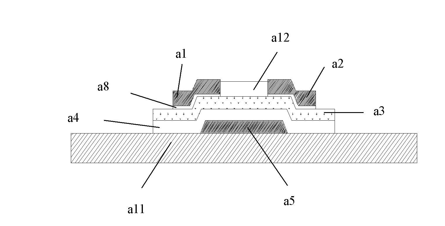
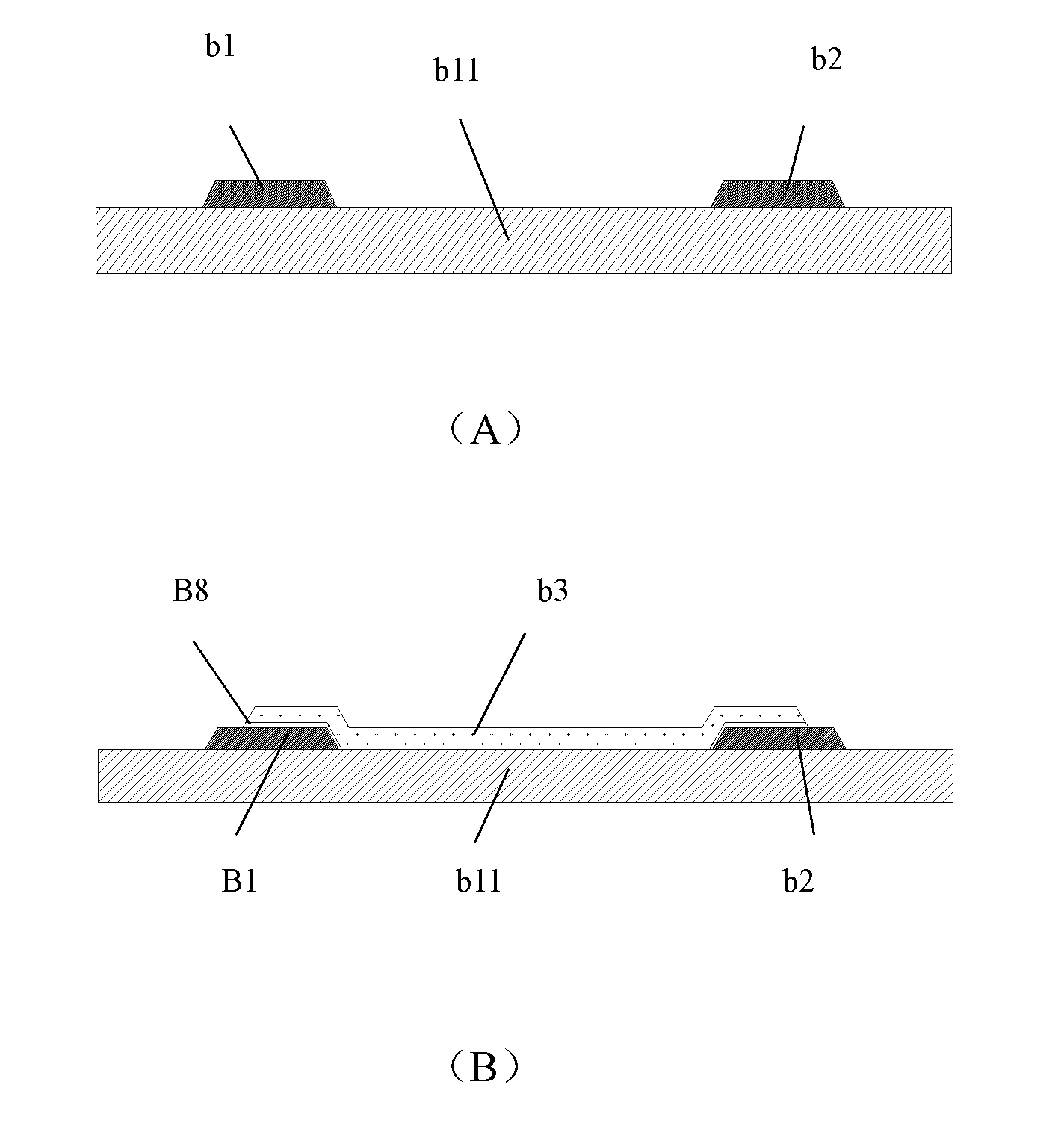
[0041] Please refer to A-G in 2, which show the process sectional view of the thin film transistor with single-gate and double-channel structure of the present invention. The thin film transistor with a single-gate double-channel structure of the present invention includes a substrate b11, a first source b1, a second source b9, a first drain b2, a second drain b10, a gate b5, and a first active layer b3, the second active layer b7; the first source b1 and the first drain b2 are formed on the substrate b11; the first active layer b3 is formed between the first source b1 and the first drain b2 between, the edges of which overlap with the edges of the first source b1 and the first drain b2; the first insulating layer b4 is formed on the first active layer b3; the gate b5 corresponds to the first active layer b3 and formed on the first insulating layer b4; the second insulating layer b6 is formed on the gate b5; the second active layer b7 corresponds to the first active layer b3 a...

Embodiment 2

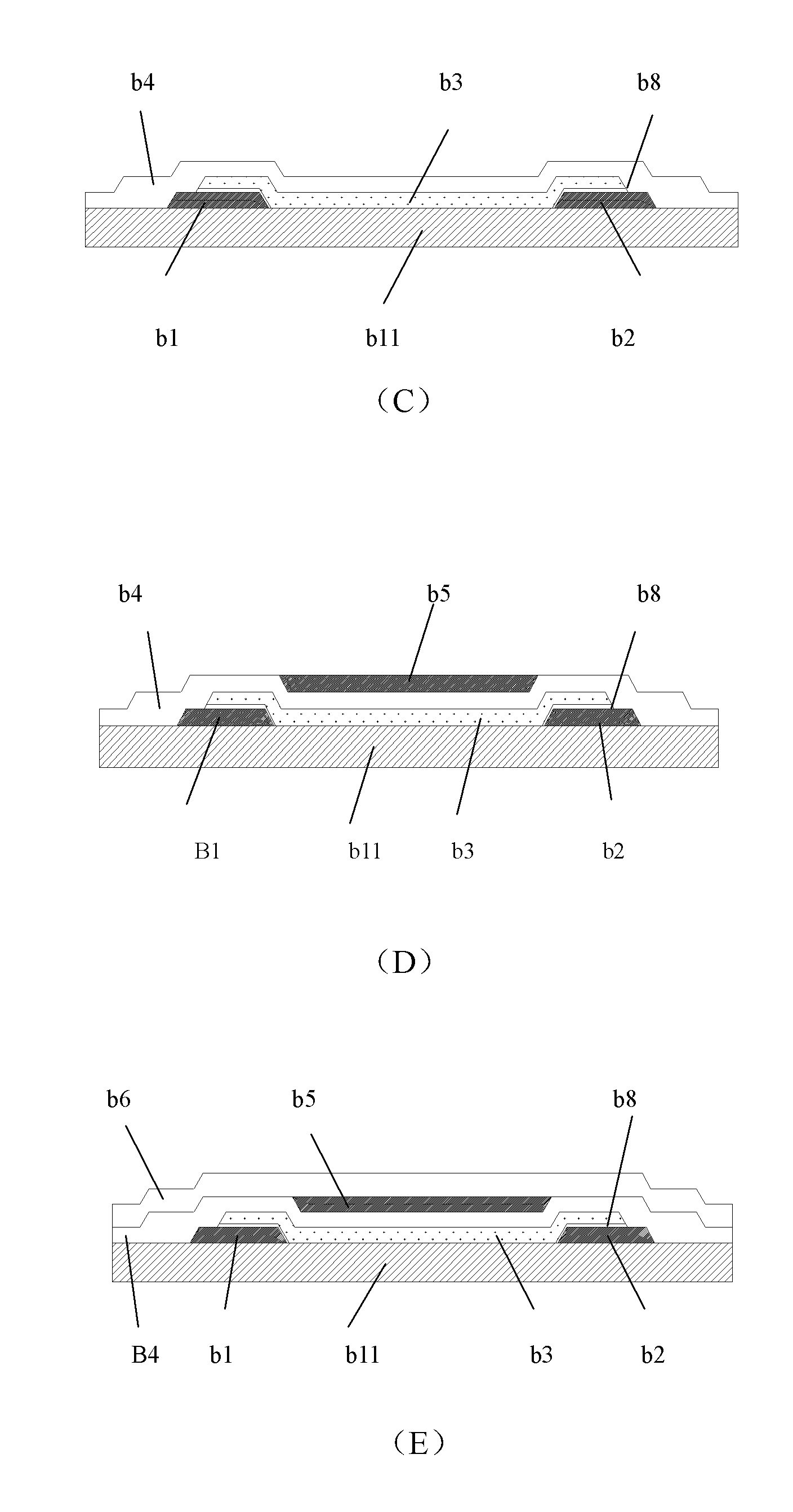
[0053] Please refer to Figs. A to G in Fig. 3, which show a cross-sectional process view of a thin film transistor with a single-gate and dual-channel structure according to Embodiment 2 of the present invention.

[0054] Such as image 3 Shown in Figure G. The thin film transistor with a single-gate double-channel structure of the present invention includes a substrate c11, a first source c1, a first drain c2, a gate c5, a first active layer c3, and a second active layer c7; The first part of the first source c1 and the first drain c2 are formed on the substrate c11; the first active layer c3 is formed between the first source c1 and the first part of the first drain c2, and its edge is in contact with the first part of the first drain c2. The edges of the first part of the first source c1 and the first drain c2 overlap; the first insulating layer c4 is formed on the first active layer c3 and the first source c1 and the first drain c2, and A through hole is left above the s...


PUM


Abstract

The invention discloses a thin film transistor with a single-gate double-channel structure and a manufacturing method thereof. The manufacturing method comprises the steps of forming a first source electrode and a first drain electrode on a base plate; depositing a first active layer, wherein the edge of the active layer is overlapped with the edges of the first source electrode and the first drain electrode; then sequentially forming a first insulation layer, a gate electrode and a second insulation layer on the first active layer; forming a second active layer on the second insulation layerin a way of corresponding to the first active layer; and forming a second source electrode and a second drain electrode on the second active layer in a way of corresponding to the first source electrode and the first drain electrode to further form the thin film transistor with the single-gate double-channel structure. The thin film transistor with the single-gate double-channel structure has the advantages that: the thin film transistor can serve as a two-way switch device or a three-state device, can be used for controlling two circuit branches with a uniform circuit behavior, has a high on state current and can serve as an inverter.

Description

technical field [0001] The invention relates to a thin film transistor and a manufacturing method thereof, in particular to a thin film transistor with a single-gate double-channel structure and a manufacturing method thereof. Background technique [0002] refer to figure 1 , which shows a cross-sectional view of a traditional single-gate single-channel thin film transistor (thin film transistor). exist figure 1 Among them, the thin film transistor a0 is basically an electronic element composed of a gate a5, a source a1, a drain a2 and an active layer a3, and an insulating layer is placed between the gate a5 and the active layer a3 separated by a4. The source a1 and the drain a2 are not in contact with each other, but are in ohmic contact with the active layer a3 through the heavily doped semiconductor layer a8 respectively. [0003] When a certain voltage is applied to the gate a5, a conductive channel is formed in the active layer a3 near the insulating layer a4. At t...

Claims


Application Information

Patent Timeline
Patent Type & Authority Applications(China)
IPC IPC(8): H01L29/786H01L29/06H01L29/08H01L29/10H01L21/336
Inventor 许志平吴为敬赖志成谢佳松颜骏
Owner 王磊
Why Eureka
Try Eureka