High-power LED (Light Emitting Diode) encapsulating structure

A LED packaging, high-power technology, applied in the direction of electrical components, electrical solid devices, circuits, etc., can solve the problems of poor particle fluidity, serious powder agglomeration, irregular shape, etc., to repair the light spot, solve the problem of light spot, improve The effect of uniformity

Inactive Publication Date: 2013-08-21
SHENZHEN OPTO CORE PHOTOELECTRIC TECH
View PDF4 Cites 0 Cited by
  • Summary
  • Abstract
  • Description
  • Claims
  • Application Information

AI Technical Summary

Problems solved by technology

At present, the most widely used yellow phosphors are YAG series phosphors. The particle size of this series of phosphors is above 17um. They have some defects, such as large particles, serious powder agglomeration, hard sample, irregular shape, and particle flow. Poor performance, etc., which is the main cause of the spot

Method used


Image

  • High-power LED (Light Emitting Diode) encapsulating structure
  • High-power LED (Light Emitting Diode) encapsulating structure
  • High-power LED (Light Emitting Diode) encapsulating structure

Examples


Embodiment 1

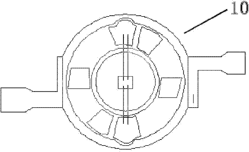
[0050]The angle α is 40°, the depth h of the bowl is 0.3mm, the LED light-emitting chip 1 is fixed on the bracket 10 with silver glue, and baked and heated to cure, wherein the chip size is 24mil×24mil; then the gold wire 2 is welded on the chip 1 Positive and negative poles; then, the fluorescent glue 7 is coated on the surface of the chip 1. In order to effectively suppress the heterochromatic aperture or light spot formed by refraction after the light passes through the lens 9, the thickness of the coating on the surface of the chip 1 is greater than that on the side of the chip, resulting in Apply fluorescent glue 7 to form an arc, the arc of which is consistent with the arc of the covered lens, and bake and shape, cover the lens 9 above the bracket, inject filling silica gel 8, and bake and shape. Magnified view of phosphor surface coating and lens coverage see Figure 7 .

Embodiment 2

[0052] The angle α is 45°, the depth h of the bowl is 0.35mm, the light-emitting chip 1 is fixed on the support 10 with silver glue, and baked and heated to cure, wherein the chip size is 38mil×38mil; then the gold wire 2 is welded on the front of the chip. , Negative electrode; then apply fluorescent glue on the surface of the chip, in order to effectively suppress the heterochromatic aperture or light spot formed by refraction after the light passes through the lens, the thickness of the coating on the surface of the chip is greater than that on the side of the chip, causing the coating of fluorescent glue 7 to form The arc shape is consistent with the arc of the covered lens, and it is baked and formed. Cover the lens 9 above the support, inject filling silica gel 8, and carry out baking molding.

Embodiment 3

[0054] The angle α is 50°, the depth h of the bowl is 0.45mm, the light-emitting chip 1 is fixed on the support 10 with silver glue, and baked and heated to cure, wherein the chip size is 45mil×45mil; , Negative electrode; then apply fluorescent glue on the surface of the chip, in order to effectively suppress the heterochromatic aperture or light spot formed by refraction after the light passes through the lens, the thickness of the coating on the surface of the chip is greater than that on the side of the chip, causing the coating of fluorescent glue 7 to form The arc shape is consistent with the arc of the covered lens, and it is baked and formed. Cover the lens 9 above the support, inject filling silica gel 8, and carry out baking molding.


PUM


Abstract

The invention discloses a high-power LED (Light Emitting Diode) encapsulating structure which comprises an LED illumination chip and an LED chip bracket, wherein the surface of the chip is coated with fluorescent glue; a lens covers above the bracket; the coating thickness of fluorescent glue on the surface of the chip is larger than that of fluorescent glue at the side edge of the chip, so that the coated fluorescent glue is in an arc with a radian accordant with that of the covered lens; the fluorescent glue is formed by adding small particles into large-particle fluorescent powder for mixing, combining the mixed fluorescent powder with silica gel, stirring for a certain period of time and performing vacuumizing treatment; the angle alpha formed by the cup wall and the cup bottom of a bracket cup is between 45 degrees and 50 degrees; and the cup height h is between 0.3 millimeter and 0.45 millimeter. By adopting the encapsulating structure, the luminescence of an LED is more uniform, the photochromic quality is effectively improved, and the problem of luminous spots is better solved.

Description

technical field [0001] The invention relates to the technical field of LEDs, in particular to a high-power LED packaging structure. Background technique [0002] LED is a light-emitting diode, which is a light-emitting device that can directly convert electrical energy into visible light and radiant energy. The structure of a light-emitting diode includes two parts: a carrying part and conductive ends of different polarities, and a chip and a fluorescent material are arranged in the carrying part. , using gold wires to connect the electrode layer and the conductive end of the chip, and finally complete the packaging process. Compared with traditional lighting technology, this new type of light source has leading advantages such as high efficiency, energy saving, long life, small size, low cost, and environmental protection. Currently commonly used LEDs mainly use the light from the chip to combine with the wavelength of the fluorescent material to form a specific light colo...

Claims


Application Information

Patent Timeline
Patent Type & Authority Patents(China)
IPC IPC(8): H01L33/48H01L33/50H01L33/60
CPCH01L2224/48091
Inventor 张奕聪曾贤平
Owner SHENZHEN OPTO CORE PHOTOELECTRIC TECH
Why Eureka
Try Eureka