Digitalized alternating-current voltage and speed regulation device

A technology of speed regulation device and AC voltage regulation, which is applied to the deceleration device of AC motor, AC motor control, emergency protection circuit device, etc. Easy to debug effects

Active Publication Date: 2011-09-14
SHANGHAI ZHIDA ELECTRONICS
3 Cites 51 Cited by

AI-Extracted Technical Summary

Problems solved by technology

This is impossible...

Method used

(2) debugging is convenient, can directly input parameter with PC by man-machine interface, or carry out parameter setting by control panel shortcut key, quick operation, shortens debugging time.
1. system adopts ATmega128 as core control device, and it has powerful compatibility and digital processing capability. Complete the software design of all logic circuits of the digital system based on AVR. Since all the information processing of the device is realized by the microprocessor, the working performance is stable. It has the advantages of high working efficiency, safety and reliability, low operating cost, easy maintenance, simple operation and convenient on-site maintenance in harsh environments. The function is more powerful, the use is more convenient, the speed regulation performance is more perfect, and the cost of the hardware is also reduced. At present, all major steel mills in the country adopt this technology, and the market prospect is very good.
2. The hardware circuit is greatly saved, the complexity of the circuit board is reduced, and the maintenance of the system is convenient. The speed feedback adopts three control modes of the tachogenerator feedback, the rotor voltage feedback and the pulse encoder feedback, and the user can according to the actual situation It is very convenient to choose.
3. adopt double closed-loop system, have good dynamic response index, the system starts and brakes smoothly, and speed regulation range is wide, is suitable for the soft start of crane speed regulation system and AC motor, and market prospect is good, and this product passes through on-site two More than a month of usage investigation, the work is stable and reliable, and the stability is good.
System CPU microprocessor chip, is to adopt the ATmega128 single-chip microcomputer that U.S. Atmel Company produces to realize, as shown in chip IC1 among Fig. 1. Its pin arrangement is shown in Figure 4. ATmega128 microcontroller is an 8-bit low-power CMOS microprocessor based on AVR RISC structure. With advanced instruction set and single-cycle instruction execution time, its data throughput rate is as high as 1MIPS/MHz, which can ease the gap between system power consumption and processing speed. contradiction. The AVR microcontroller core has a rich instruction set and 32 general-purpose working registers, all of which are directly connected to the arithmetic logic unit (ALU), so that one instruction can simultaneously access two independent registers within one clock cycle. This structure greatly improves code efficiency and has a data throughput 10 times higher than ordinary complex instruction set microprocessors.
The effect of differential link is to stop the change of deviation, and it is to control according to the variation trend (change speed) of deviation. The faster the deviation changes, the larger the output of the differential controller and can correct the deviation before it becomes large. The introduction of the differential action will help to reduce the overshoot, overcome the oscillation, and make the system tend to be stable, especially for high-order systems, which speeds up the tracking speed of the system. However, the function of differentiation is very sensitive to the noise of the input signal. Generally, no differentiation is needed for those systems with large noise, or the input signal is filtered before the differentiation works.
There is the shortcoming of complex circuit structure in the variable M/T method measuring circuit that is made of discrete devices, except resistance, electric capacity, also need multichip gate circuit, flip-flop, peripheral chip etc., device is many, and power consumption is big. It is easily disturbed by external noise and has poor reliability. This system uses ATMega8 as the core to complete the signal processing of the speed feedback of the photoelectric encoder, which simplifies the circuit design. Then communicate the processed data with ATMega128 through the serial port.
This design is a digital development on the basis of our company's original analog voltage regulation and speed regulation system KJT-400, and the system hardware diagram is as shown in Figure 1. Its control principle is to change the stator voltage of the motor. According to the principle of electromechanics, the square of the stator voltage of the motor is proportional to the torque. The control device changes the stator voltage of the motor by changing the phase shift angle of the thyristor to achieve the purpose of speed regulation. . In order to improve the hardness of the mechanical properties of the system and limit the starting and braking current of the motor, uniform acceleration and deceleration can be realized. The system design adopts a double closed-loop control system, that is, the outer loop is a speed loop, and the inner loop is a current loop, which is realized by software. The power supply provides energy to the motor through the thyristor power module, so that the motor generates torque. According to the required speed reference value, the controller controls the phase shift angle of the thyristor, changes the stator voltage of the motor, and changes the torque of the motor. The speed closed-loop system is formed by means of speed feedback devices such as tachogenerators and pulse encoders to achieve constant speed. The controller controls the voltage of the thyristor power module and controls the switching of the rotor resistance by controlling the on-off of the contactor, and optimizes the torque-speed characteristic to achieve optimal control. The reversal of the motor is achieved by changing the phase sequence of the motor. The braking of the motor is achieved by reverse braking.
[0092] The thyristor used in this design is a one-way thyristor module produced by IXYS Company, and each module is composed of two thyristors. The main circuit of this product uses five thyristor modules, which realizes the high integration of high-power semiconductors, reduces the investment in electronic circuit circuit design, and saves space.
[0101] It can be seen that when the slip rate s is constant, the electromagnetic torque is proportional to the square of the stator voltage, which sho...

Abstract

The invention provides a digitalized alternating-current voltage and speed regulation device. The digitalized alternating-current voltage and speed regulation device comprises an input signal interface circuit and an output signal interface circuit of a power circuit, a pulse trigger circuit, a key and menu display circuit and singlechips ATmega128 and ATmega8. According to the requirements of the present market and the on-site use environment, a full-digital voltage and speed regulation system is developed based on the original analog quantity voltage and speed regulation system. The system has the following basic functions: (1) due to digitalized control, the stability of the system is enhanced, and drifting of parameters due to null shifting of an amplifier and vibration of a potentiometer can be avoided; 2) the system is convenient to debug, the parameter can be directly input by using a personal computer (PC) through a human-machine interface or the parameter can be configured bya shortcut key of a control panel, the operation is quick and the debugging time can be shortened; 3) the human-machine interface monitors working states such as current, voltage, speed and the like during running of a motor in real time; and 4) by fault self-diagnosis and memory monitoring functions, the control panel displays a type code of a fault when the system is faulted, so that a user canfind out the fault conveniently.

Application Domain

AC motor controlEmergency protective circuit arrangements +2

Technology Topic

PotentiometerSelf-diagnosis +10

Image

  • Digitalized alternating-current voltage and speed regulation device
  • Digitalized alternating-current voltage and speed regulation device
  • Digitalized alternating-current voltage and speed regulation device

Examples

  • Experimental program(1)

Example Embodiment

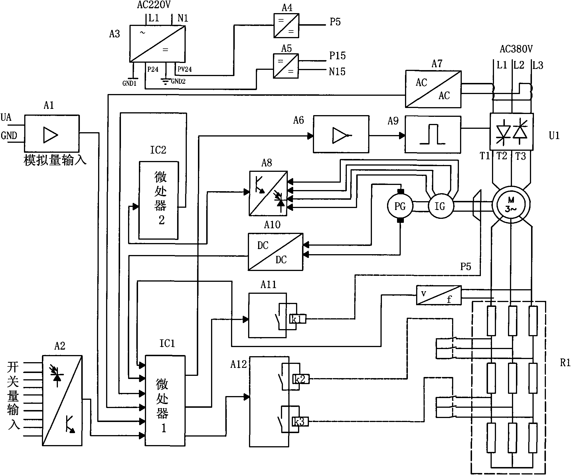
[0069] In order to make the technical means, creative features, objectives and effects of the present invention easy to understand, the preferred embodiments of the present invention are given below in conjunction with the accompanying drawings to illustrate the technical solutions of the present invention in detail.
[0070] 1. Overall design plan
[0071] 1.1 System function
[0072] Based on the requirements of the current market and on-site use environment, a fully digital voltage and speed control system is developed on the basis of the original analog voltage and speed control system. The basic functions of the system are as follows:
[0073] (1) Digital control can improve the stability of the system and avoid parameter drift caused by zero drift of the amplifier and vibration of the potentiometer.
[0074] (2) It is convenient to debug. You can directly input parameters through the man-machine interface with a PC, or set the parameters through the shortcut keys on the control panel, which can quickly operate and shorten the debugging time.
[0075] (3) The man-machine interface monitors the current, voltage, speed and other working conditions of the motor in real time.
[0076] (4) There are fault self-diagnosis and memory monitoring functions. When a fault occurs, the fault type code is displayed on the control panel, which is convenient to find the fault.
[0077] The main technical indicators are:
[0078] (1) Speed ​​adjustment range: D=20:1 (D is the ratio of the maximum speed to the minimum speed)
[0079] (2) System static error rate: ≤5%
[0080] (3) Current loop step response: ≤100ms
[0081] (4) Speed ​​loop step response: ≤500ms
[0082] 1.2 Overall system design
[0083] This design is a digital development on the basis of our company’s original analog voltage regulation system KJT-400. figure 1 Shown. The control principle is to change the stator voltage of the motor. According to the principle of electrical engineering, the square of the stator voltage of the motor is proportional to the torque. The control device changes the stator voltage of the motor by changing the phase shift angle of the thyristor to achieve the purpose of speed regulation. . In order to improve the mechanical characteristic hardness of the system and limit the starting and braking current of the motor, realize uniform acceleration and deceleration. The system design adopts a double closed loop control system, that is, the outer loop is a speed loop, and the inner loop is a current loop, which is realized by software. The power supply provides energy to the motor through the SCR power module to make the motor generate torque. The controller controls the phase shift angle of the thyristor according to the required speed reference value, changes the stator voltage of the motor, and changes the torque of the motor. A speed closed loop system is formed through speed feedback devices such as tachogenerators, pulse encoders, etc., to achieve constant speed. The controller controls the voltage of the SCR power module and controls the switching of the rotor resistance by controlling the on and off of the contactor, and optimizes the torque-speed characteristics to achieve optimal control. The reversal of the motor is achieved by changing the phase sequence of the motor. The braking of the motor is realized by reverse braking.
[0084] 1.3 Main difficulties of the system
[0085] (1). Establish a new mathematical model
[0086] Since the control system is converted from analog to digital, the stability of the automatic control system must be calculated, and the current regulator, speed regulator, ramp generator, and various protection functions in the original system must be converted into corresponding The mathematical model is realized by software through algorithms. The new mathematical model is used to supplement the required data volume to provide a digital foundation for the analysis of static parameters, dynamic response, protection functions, and man-machine interface.
[0087] (2). Research on man-machine interface
[0088] Research how to develop dynamic man-machine interface, parameter setting, motor parameter monitoring, fault display memory and other issues, and enhance the flexibility and monitorability of man-machine interface.
[0089] 2. The composition of the system:
[0090] 2.1 Main circuit
[0091] The main circuit of this design uses a thyristor double pulse trigger circuit to control the motor, such as figure 1 Shown in U1 module. The actual connection circuit such as figure 2 As shown, five pairs of thyristors are connected in anti-parallel in series on each phase winding. Phase control is used for voltage regulation. When the load current flows, at least one phase of the forward thyristor and the other group of reverse thyristors must be turned on at the same time, so just like the three-phase bridge rectifier circuit, the trigger pulse width of each thyristor is required Both should be greater than 60°, or use double pulse trigger. Using double-pulse trigger circuit, the output voltage waveform is not a sine wave when phase shifting and voltage regulation. Analysis shows that the output voltage does not contain even harmonics, and the third harmonic is the main component of the odd harmonics. If the motor winding does not have a neutral wire, although the third harmonic electromotive force exists, there will be no third harmonic current. Because the motor winding is an inductive load, the current waveform will be smoother than the voltage waveform, but it still contains harmonics, resulting in impulse torque and additional loss and other adverse effects. This is the shortcoming of the thyristor voltage regulator circuit. When the motor is running in forward and reverse rotation, in addition to the thyristors 1-6 that work in the forward rotation, the thyristors 7-10 that supply the reverse phase sequence power supply are still required. Together with 1 and 4, they can realize the reverse operation. This circuit can also realize reverse braking and dynamic braking of the motor. When reverse braking, the working thyristors are the six devices mentioned above that work in reverse. When dynamic braking is required, a few thyristors can be selected to work asymmetrically according to the form of the braking circuit. For example, let the three devices 1, 2, and 6 turn on, and all other devices will be turned off to make the motor stator The direct current flows through the windings, and it brakes against the rotating motor rotor.
[0092] The thyristor used in this design is a unidirectional thyristor module produced by IXYS Company, and each module is composed of two thyristors. The main circuit of the product adopts five thyristor modules, which realizes the high integration of high-power semiconductors, reduces the investment in electronic circuit circuit design, and saves space.
[0093] 2.2 AC motor circuit
[0094] This design adopts three-phase asynchronous winding motor, and adopts the design method of voltage regulation and speed regulation in slip power consumption type speed regulation. The voltage regulation principle is: According to the mechanical characteristic equation of the asynchronous motor
[0095] T = 3 p U 1 2 R 2 / S ω 1 [ ( R 1 + R 2 / S ) 2 + ω 1 2 ( L 11 + L 12 ) 2 ] Formula (2-1)
[0096] Where p-the number of pole pairs of the motor;
[0097] U 1 , Ω 1 -Motor stator phase voltage and power supply angular frequency;
[0098] S-slip rate;
[0099] R 1 , R 2 -The stator resistance per phase and the rotor phase resistance converted to the stator side;
[0100] L 11 , L 12 -Leakage inductance of each phase of the stator and the leakage inductance of each phase of the rotor converted to the stator side.
[0101] It can be seen that when the slip rate s is constant, the electromagnetic torque is proportional to the square of the stator voltage, which means that different stator voltages can obtain a set of different man-made mechanical characteristics, such as image 3 a. With constant torque load T L When, different stable speeds can be obtained, such as image 3 Lines A, B, and C in a. Since the slip rate s of the working section of the ordinary asynchronous motor is very small, in order to expand the variable voltage speed regulation range under a constant torque load, the motor must run stably at a lower speed without overheating, and the rotor winding of the motor is required to be relatively high. High resistance value. image 3 b. The mechanical characteristics of the high rotor resistance motor at variable voltage are given. Obviously, the range of variable voltage and speed regulation under constant torque load is increased. Moreover, the motor will not be burnt when working under the locked-rotor torque. Therefore, this device requires that when the motor is running with a load, the rotor should always be connected in series with a resistor, so that the motor will not burn out when the motor is overheated and locked at low speed.
[0102] 2.3 Speed ​​feedback loop
[0103] The design of this device is a double closed loop speed control system with speed closed loop and current closed loop. The speed feedback method adopts three methods: pulse encoder, tachogenerator, and rotor frequency feedback. Among them, pulse encoder and tachogenerator feedback methods have high precision, which is suitable for occasions requiring high precision. The rotor frequency feedback method is simple to apply, no need to add a speed sensor, cost saving and easy to use. Its control accuracy and performance are worse than the previous two methods. It can be used in occasions where the speed accuracy is not high. Users can choose according to actual needs.
[0104] 2.3 System microprocessor hardware chip
[0105] The system CPU microprocessor chip is realized by the ATmega128 single chip microcomputer produced by American Atmel company, such as figure 1 The middle chip is shown in IC1. The pins are arranged as Figure 4 Shown. The ATmega128 microcontroller is an 8-bit low-power CMOS microprocessor based on the AVR RISC structure. With its advanced instruction set and single-cycle instruction execution time, its data throughput rate is as high as 1MIPS/MHz, which can ease the system's power consumption and processing speed. Contradiction. The AVR microcontroller core has a rich instruction set and 32 general-purpose working registers. All registers are directly connected to the arithmetic logic unit (ALU), so that one instruction can simultaneously access two independent registers within one clock cycle. This structure greatly improves code efficiency and has a data throughput that is 10 times higher than that of an ordinary microprocessor with a complex instruction set.
[0106] Built-in ATmega128 microcontroller: 128KB of in-system programmable Flash program memory, with the ability to read during writing, that is, simultaneous read and write (RWW); 4KB of EEPROM; 4KB of SRAM; 53 general-purpose I/O port lines ; 32 general-purpose working registers; real-time clock (RTC); 4 flexible timers/counters (T/c) with comparison mode and PWM function; 2 UJSART; byte-oriented two-wire interface (TWI); 8 Channel 10-bit ADC; optional programmable gain; programmable watchdog timer of on-chip oscillator; serial peripheral interface (SPI); JTAG test interface compatible with IEEE1149.1 specification, this interface can also Used for on-chip debugging; 6 power saving modes that can be selected by software. CPU stops working in idle mode, while SRAM, T/C, SPI port and interrupt system continue to work; crystal oscillator stops oscillating in power-down mode, all functions except interrupt and hardware reset stop working, and the contents of the register are always Keep; the asynchronous timer continues to run in the power-saving mode to allow the user to maintain the time base, and other parts of the device are in a sleep state; when the ADC noise is always mode, the CPU and all I/O modules stop running, while the asynchronous timer and ADC Continue to work to reduce the switching noise during ADC conversion; in Standby mode, the oscillator works, while other parts sleep, so that the device consumes very little current and has a fast start-up capability; expanded Standby mode allows vibrators and asynchronous timers continue working. The device is produced with Atmel's high-density non-volatile memory technology. The on-chip ISP Flash can be programmed multiple times through SPI interface, universal programmer, or bootloader. The boot program can use any interface to download the application program to the application Flash memory. When the application Flash memory is updated, the program in the boot Flash area continues to implement the RWW operation. By integrating the 8-bit RISC CPU and the programmable Flash in the system into one chip, ATmega128 provides a flexible and low-cost solution for many embedded control applications. ATmega128AVR has a complete set of development tools, including C compiler, macro compiler, program debugger, emulator and evaluation board. The A/D conversion processing of the feedback loop of the tachogenerator is processed by the internal A/D converter of the ATmega128 chip. The data processing of the pulse encoder is realized by the microcontroller ATmega8 chip.
[0107] 2.4 System development environment
[0108] 2.4.1 Hardware development environment
[0109] The hardware that the control system needs to design mainly include: main control circuit board, pulse circuit board, display control circuit board. Here, Protel 99 is selected as the hardware development environment.
[0110] Protel is a product of Protel Technology. Protel 99 is a 32-bit EDA design system based on the Windows platform. It has rich and diverse editing functions, powerful and convenient automatic design capabilities, perfect and effective testing tools, flexible and orderly design management methods, and good openness also makes it Can be compatible with multiple formats of design files. Protel 99 also supports all output peripherals on the Windows platform and provides high-resolution light drawing files so that users can easily control the entire process of electronic circuit design.
[0111] 2.4.2 Software Development Environment
[0112] 2.4.2.1 Introduction to AVR CPU Core
[0113] In order to get the maximum degree of performance and parallelism, AVR uses the Harvard structure, the block diagram of the structure is as follows Figure 5 Shown.
[0114] Have independent data and program buses. The instructions in the program memory are run through a one-stage pipeline. The CPU reads the next instruction while executing one instruction. This concept realizes the single clock cycle operation of instructions. The program memory is FLASH which can be programmed online. The quick access register file includes 32 8-bit general-purpose working registers, and all of them can be accessed within one clock cycle. So as to realize the ALU operation of a single clock cycle. In a typical ALU operation, two operands located in the register file are accessed at the same time, and then the corresponding operation is performed, and the result is sent back to the register file. The whole process only needs one clock cycle.
[0115] There are 6 registers in the register file that can be used as 3 16-bit indirect address register pointers to address the data space to achieve efficient address operations. One of the pointers can also be used as the address pointer of the program memory look-up table. These additional function registers are 16-bit X, Y, and Z registers. ALU supports arithmetic and logical operations between registers and between registers and constants. ALU can also perform single register operations. After the operation is completed, the contents of the status register will be updated to reflect the operation result.
[0116] The program flow is controlled by jump instructions and call instructions with/unconditional, thereby directly addressing the entire address space. Most instructions are 16 bits in length, that is, each program memory address contains a 16-bit or 32-bit instruction.
[0117] The program storage is divided into two empty areas, the boot program area and the application program area, both of which are specifically positioned to achieve read and read/write protection. The SPM instruction used to write the application program area must be located in the boot program area.
[0118] The return address program counter (PC) is stored in the stack when interrupting and calling a subroutine. The stack is located in the general data SRAM, so its depth is only limited by the size of the SRAM. In the reset routine, the user must first initialize the stack pointer SP. This pointer is located in the I/O space and can be read and written. The data SRAM can be accessed through 5 different addressing modes.
[0119] The AVR memory space is a linear planar structure.
[0120] AVR has a flexible interrupt module. The control register is located in the I/O status register with a global interrupt enable bit. There is an interrupt vector table at the beginning of the program memory, and each interrupt has an independent interrupt vector here. The priority of each interrupt is related to its position in the interrupt vector table. The lower the interrupt vector address, the higher the priority.
[0121] The I/O memory space contains 64 addresses that can be directly addressed. Mapped to the data space is the address $20_$5F after the register file. In addition, ATmega128 has expanded I/O space in SRAM,
[0122] 2.4.2.2 Features of ICCAVR:
[0123] Since the main chip of the system control circuit is ATmega128, the software development environment of the control system is ICCAVR.
[0124] Since the birth of ATMEL’s AT90 series microcontrollers, many third-party manufacturers have developed C language tools for program development for the AT90 series. ICCAVR is one of the third-party C compilers recommended by ATMEL. ICCAVR is a tool that conforms to the ANSI standard C language to develop MCU programs. It has suitable functions, convenient use, and good technical support. It has the following characteristics:
[0125] 1).ICCAVR is an integrated working environment (IDE) that integrates editor and project manager;
[0126] 2). All source files are organized into projects, file editing and project construction are also completed in this environment, errors are displayed in the status window, and when you click the compilation error, the cursor automatically jumps to the wrong one One line
[0127] 3). The project manager can also directly generate INTEL HEX format files that can be used directly, which can be supported by most programmers for downloading to the chip;
[0128] 4).ICCAVR is a 32-bit program that supports long file names.
[0129] C language is a structured language that can produce compact codes. Compared with assembly language, it has the following advantages:
[0130] ① It is not required to understand the instruction system of the microcontroller, only a preliminary understanding of the memory structure;
[0131] ② Details such as register allocation, addressing of different memories and data types can be managed by the compiler;
[0132] ③The program has a standardized structure and can be divided into different functions. This way can make the program structured;
[0133] ④It has the ability to combine variable selection with special operations, which improves the readability of the program;
[0134] ⑤Keywords and calculation functions can be used in a way that approximates human thinking;
[0135] ⑥The time of programming and program debugging is significantly shortened, thereby improving efficiency;
[0136] ⑦The provided library contains many standard subroutines and has strong data processing capabilities;
[0137] ⑧The programmed program can be easily inserted into the new program, because it has convenient modular programming technology.
[0138] 3. System hardware design and implementation
[0139] 3.1 The composition of the control system
[0140] The control system is mainly composed of power supply circuit, input signal interface circuit, output signal interface circuit, pulse trigger circuit, button and menu display circuit, and single-chip ATmega128 and ATmega8. The input signals include switch signal, analog signal and speed feedback digital signal; the output signal is mainly to control the contactor switching resistance and comprehensive fault alarm; the pulse from the single-chip microcomputer controls the output of the thyristor; the button and menu display circuit The system parameters can be set on the board, and the fault information can be displayed through the fault display code. See the block diagram of the control system figure 1 Shown.
[0141] 3.2.1 Power supply circuit design
[0142] In order to ensure that the device has good anti-interference ability and improve the stability of the system, the power circuit adopts two independent DC24V power supplies to play the role of external input interface and internal isolation. The power supply of this control system is mainly divided into the external switch input part DC24V1, and the internal DC24V2 as the working voltage of the relay and pulse trigger part, the ±15V required by the peripheral chip and interface circuit, and the +5V working voltage of the single-chip microcomputer. The principle block diagram of the power circuit is as figure 1 As shown in the figure, the A1 module in the figure adopts AC220V input, and outputs two independent DC power supplies, P24 and PV24, two 24V DC power supplies through transformer step-down, rectification, filtering, and output. Among them, PV24 outputs 5 volts voltage P5 through DC/DC conversion module A4 to supply power to the microcontroller. P24 passes through the DC/DC converter module A5 to output a positive 15V power supply P15 and a negative 15V power supply N15 to supply power to the peripheral chip interface circuit. The schematic diagram of the power circuit is as follows Image 6 Shown.
[0143] The function of the power transformer is to convert the 220V AC voltage of the grid into the AC voltage required by the rectifier and filter circuit. The rectifier bridge converts the AC voltage into a pulsating DC voltage. After capacitor filtering, after the module power conversion, the required circuit operating voltage is obtained. .
[0144] 3.2.2 Input signal interface circuit design
[0145] 3.2.2.1 Switch interface circuit design
[0146] Switch input signals, mainly including zero position, stop, 2 direction signals and 3 speed gear signals from the master commander, limit signals, over temperature, overload and brake fault signals, etc. contact signals; through photoelectric Coupling module A2, to the input of microprocessor module IC1 for signal processing, the circuit block diagram is as follows figure 1 Shown. The circuit schematic diagram is as Figure 7 Shown.
[0147] The contact signal of the switch input, through the X2:1 terminal and the light-emitting diode and the current limiting resistor R9 to the input end of the optical coupler CNY17-2. When the X2:1 terminal is at a high level, the light-emitting diode DS1 is turned on through the photoelectric coupling transistor, and the emitter outputs a high level as the input signal of the single-chip microcomputer. The LED DS1 is displayed as an input signal.
[0148] Since the input and output of the optocoupler are isolated from each other, and the electrical signal transmission has the characteristics of unidirectionality, it has good electrical insulation and anti-interference capabilities. In addition, since the input end of the optocoupler is a low-resistance element that works in current mode, it has a strong common-mode rejection capability. Therefore, it can greatly improve the signal-to-noise ratio as a terminal isolation element in long-line transmission of information. As a signal isolation interface device in computer digital communication and real-time control, it can greatly increase the reliability of computer work. The main advantages of optocouplers are: signal one-way transmission, the input end and the output end are completely electrically isolated, the output signal has no effect on the input end, strong anti-interference ability, stable operation, no contact, long service life, and transmission High efficiency, in order to improve the optocoupler transmission ratio, the choice of resistor R9 should ensure that the optocoupler input current is above 10mA.
[0149] Therefore, the isolation function of the optocoupler is used here to provide a reliable input signal for the microcontroller. This signal is a high level of +5V, or a low level of 0V.
[0150] 3.2.2.2 Analog signal interface circuit design
[0151] 1. Analog speed setting circuit
[0152] The analog speed setting is stepless speed regulation. The potentiometer coaxial with the operating handle is used as the speed setting. The input voltage is 0~±10 relative to the rated speed of 0~100%. The analog quantity speed given signal is input by the A1 module, and sent to the A/D converter inside the single-chip microcomputer through calculation to convert the analog quantity into a digital quantity, which is processed and controlled by the CPU. see figure 1 The system block diagram is shown. This system is designed with three consecutive given input terminals that can be used to connect external given signals, and all input terminals can be input with ±10V voltage. Interface circuit diagram such as Figure 8 Shown:
[0153] The ±10V voltage signal input for a given analog speed, after being acted by the follower U26B amplifier, and the 2.5V standard voltage generated by the follower U26A, are simultaneously sent to the adder U26D to obtain a 0~2.5V voltage signal, which is input to the microcontroller Inside, A/D conversion is carried out in the microcontroller.
[0154] 2. Current feedback circuit design
[0155] The current feedback loop mainly provides the current feedback value of the current regulator to form a current loop and provide over-current protection. This value is sent to the single-chip microcomputer and processed by software. The principle is shown in Figure 9(a), through the current transformer secondary resistance T1 , T2, detect the actual value of the main loop current, obtain the voltage drops u1 and u2 through the R1 and R2 resistors, and input them to the amplifier for processing, as shown in Figure 9(b), the amplifier U19C detects the L1 phase current, and the amplifier U19A detects the L3 phase current , Through the amplifier U19B and U19B superimposed, the output current feedback value to the single-chip microcomputer.
[0156] Because the ADC reference voltage source REF in the microcontroller ATmega128 is 2.56V, the I-back should be less than this voltage value, because when the motor starts, the starting current will reach about twice the rated current, so when determining the feedback resistance, Consider the size of the starting current. The transformation ratio of the current transformer is designed such that when the system reaches the rated current, the secondary side current of the transformer is 1A, and the sampling resistance R1 and R2 is 1 ohm, then u1 and u2 are 1V. The value calculated into the microcontroller is as follows:
[0157] I - back = ( 8.2 K 10 K * 1 V ) * ( 1 K + 1 K 2 K ) Formula (3-1)
[0158] = 1.23 V
[0159] 3. Speed ​​feedback circuit design
[0160] The speed feedback mode of this device is divided into three forms: tachogenerator speed feedback, pulse encoder speed feedback, and rotor frequency feedback. This section mainly describes the use of tachogenerator as the input circuit of the speed detection element. When the speed of the commonly used tachogenerator is 1000RPM, the output voltage is 100V or 60V, so an attenuation circuit is needed. The circuit design uses resistor divider to obtain the speed feedback voltage. The input circuit block diagram is as follows figure 1 Shown. The voltage detected by the tachogenerator is input to the microcontroller module IC1 for A/D conversion via the attenuation module A10. The actual circuit is shown in Figure 10(a). According to the different output voltages of the tachogenerator and the number of revolutions of the driving motor, the microprocessor controls the electronic switch to short-circuit the resistance on the regulating board to obtain the feedback signal of the tachogenerator. For a 100V/1000 rpm tachogenerator, do not short-circuit for 4-pole motors; short-circuit R74 and R61 for 6-pole motors; short-circuit R74, R61 and R54 for 8-pole motors; short-circuit R74, R61, R54 and R46 for 10-pole motors . For a 60V/1000 rpm tachogenerator, 4-pole short-circuit R74 and R61, 6-pole short-circuit R74, R61 and R54, and 8-pole short-circuit R74, R61, R54 and R46.
[0161] In this way, -12V≤Ui≤+12V is obtained. Ui enters the follower first, and then superimposes the signal with the given 2.5V. The feedback speed speadback is obtained through an inverted proportional operational amplifier circuit. The schematic diagram is shown in Figure 10(b), and the calculation formula is:
[0162] speedback = - 10 K 10 K [ ( - 2.5 K 5 K ) * 2.5 V + ( - 2.5 K twenty four K ) * Ui ] Formula (3-2)
[0163] Thus, the input signal of 0 ~ 2.5V can be obtained.
[0164] 4. Rotor voltage feedback
[0165] According to the principle of AC asynchronous motor, the rotor voltage of the motor is proportional to the rotor frequency and inversely proportional to the motor speed. By sampling the rotor voltage signal as the speed feedback signal, the same function as the tachogenerator can be realized. The accuracy and performance of this control method are slightly inferior to that of tachogenerator and pulse encoder feedback methods. It can be used in occasions where the control accuracy is not high. Users can choose according to actual conditions. The control principle is like figure 1 As shown, the two-phase voltage is taken from the motor rotor, processed by the f/v frequency-voltage conversion module, and converted into a voltage signal proportional to the speed, and sent to the single-chip module C1 for processing.
[0166] 3.2.2.3 The realization of ATmega128's analog to digital conversion
[0167] The signal from the encoder and the tachogenerator is a voltage signal of 0 ~ 2.5V. We know that the single-chip microcomputer needs to process a digital signal of 0 or 1, so before the single-chip microcomputer processes the continuous input speed feedback, the The input analog signal is digitally converted.
[0168] The ADC analog/digital conversion process mainly includes two parts. First, sample and save the data to be converted, and then quantify the collected data. In this way, the data conversion is completed. The purpose of sampling is to collect the original data one by one. Therefore, the higher the sampling rate, the less likely the signal is to be distorted, that is, the higher the resolution. The purpose of quantization is to encode the data obtained by sampling with a combination of 0 and 1 , The higher the number of bits of the same quantization, the higher the resolution.
[0169] (1) ADC conversion
[0170] ATmega128 has a 10-bit successive approximation line ADC. The ADC is connected to an 8-channel analog multiplexer, which can sample 8-channel single-ended input voltages from the port. Single-ended voltage input is subject to 0V (GND). ADC includes a sample and hold circuit to ensure that the voltage input to the ADC remains constant during the conversion process. The ADC converts the input analog voltage into a 10-bit digital quantity through successive approximation methods. The minimum value represents GND, and the maximum value represents the voltage on the AREF pin minus 1LSB. AVCC or the internal 2.56V reference voltage can be leveled to the AREF pin through the REFSn bit of the ADMUX register. An external capacitor on AREF can decouple the on-chip reference voltage to improve noise suppression performance.
[0171] (2) To frequency division and conversion timing
[0172] Under default conditions, the successive approximation circuit requires an input clock from 50KHZ to 200KHZ to obtain maximum accuracy. If the required conversion accuracy is less than 10 bits, the input clock frequency can be higher than 200KHZ to achieve a higher sampling rate. The ADC module includes a prescaler, which can generate an acceptable ADC clock from any CPU clock over 100HZ. Frequency divider such as Picture 11 Shown.
[0173] Normal conversion requires 13 ADC clock cycles. In order to initialize the analog circuit, the first conversion after the ADC is enabled requires 25 ADC clock cycles. In the ordinary ADC conversion process, the sample and hold starts at 1.5 clocks after the start of the conversion, and the sample and hold of the first ADC conversion occurs 13.5 ADC clocks after the start of the conversion. After the conversion, the ADC result is sent to the ADC data register. In continuous conversion mode, when ADSC is 1, as long as the conversion ends, the next conversion will start immediately. Conversion timing diagram such as Picture 12 Shown.
[0174] (3) ADC analog input channel
[0175] Single-ended channel analog input circuit such as Figure 13 As shown, whether it is used as an ADC input channel or not, the analog signal input to ADCn is affected by pin capacitance and input leakage. When used as an ADC input channel, the analog signal source must drive the sample and hold (S/H) capacitor through a series resistor (combined resistance of the input channel). ADC is optimized for analog signals whose output impedance is close to 10KΩ or less. The sampling time for such a signal can be ignored. If the signal has a higher impedance, then the sampling time depends on the time to charge the S/H capacitor. This time may vary greatly.
[0176] (4) ADC accuracy definition and error
[0177] An n-bit single-ended ADC converts the linear voltage between GND and VREF into 2 n (1LSB) different digital quantities. The smallest conversion code is 0, the largest conversion code is 2 n -1. The result of a single conversion is as follows:
[0178] ADC = V IN · 1024 V REF Formula (3-3)
[0179] Where V IN Is the input voltage of the selected pin, V REF It is the reference voltage.
[0180] Quantization error: Since the input voltage is quantized into a limited number of bits, a certain range of input voltage (1LSB) is converted to the same number, and the quantization error is always ±0.5LSB.
[0181] Absolute accuracy: The maximum deviation between all actual conversions (unadjusted) and theoretical conversions. It consists of offset, gain error, differential error, nonlinearity and quantization error, and the ideal value is ±0.5LSB.
[0182] 3.2.2.4 Digital signal interface circuit
[0183] The ways and means to realize speed feedback have a great influence on the steady-state error and dynamic response performance of the system. For a high-precision control system, it is required to achieve high-resolution, stable and accurate accuracy in a large speed range. Speed ​​feedback. The traditional analog quantity as the speed feedback parameter system, due to the influence of factors such as nonlinearity, temperature change and component aging, it is difficult to meet the requirements of rapidity and accuracy in the control process. Encoder is a device that completes feedback with digital quantities. It can directly interface with the microcomputer. Such as figure 1.1 As shown in the block diagram, the pulse encoder IG coaxial with the motor, the pulse generated when the motor rotates is processed through the photoelectric coupling module A8 to the input of the single-chip microcomputer module IC1.
[0184] The schematic block diagram of the feedback control using the photoelectric encoder is as follows Figure 14 As shown,
[0185] 1. The principle of encoder speed measurement
[0186] The photoelectric encoder is directly connected with the motor spindle, so that the encoder and the motor spindle are completely consistent. Its working principle is that the photoelectric encoder rotates with the motor and produces two phases (phase A, phase B) with a difference of 90 in proportion to the speed. Quadrature encoding pulse of phase angle. If the A-phase encoding pulse is ahead of the B-phase encoding pulse, the photoelectric encoder rotates forward, otherwise it is reverse. Phase A is used to measure the number of pulses. Phase B and Phase A are used to measure the direction of rotation, so that the motor speed and steering can be measured. The photoelectric encoder outputs fewer pulses at low speed, and it is difficult to ensure accuracy in general application. In order to improve the measurement accuracy and resolution, in addition to selecting a high-resolution encoder, the output of the encoder can also be subdivided in multiple frequencies, and then a counter can count the generated multiple-frequency pulse signals. Through the measurement time T and the count value M of the measured pulse signal by the counter within T. After calculation, the motor speed can be determined. The speed given data is sent by the main control computer, and compared with the actual measured speed data, the control system outputs the control parameters according to the comparison result, and completes the closed loop control of speed feedback.
[0187] 2. Commonly used speed measurement methods
[0188] There are three commonly used speed measurement methods: T method, M method and M/T method. The T method determines the speed by measuring the time interval between the two phase pulses of the encoder. This method is less accurate when the speed is high, and is generally suitable for low speed occasions: the M method is to measure the encoder for a fixed period of time. The number of pulses is used to determine the speed, which is suitable for high-speed occasions; while the M/T law is a combination of the first two methods and has good accuracy in the entire speed range. However, in order to ensure the accuracy of the results at low speeds, this method requires a long detection time, which cannot meet the fast dynamic response indicators of the speed detection system. Therefore, the variable M/T speed measurement method and the variable M/T speed measurement method have appeared The schematic diagram is as Figure 16 As shown,
[0189] The so-called variable M/T method refers to the detection of the count pulse M of the photoelectric encoder during the speed measurement process. d , Also detect the high frequency clock pulse M t , The detection time T is always equal to M d The sum of pulse signal periods. M d The number can be preset, but obviously the detection time T is not fixed, and T decreases as the speed increases. The measuring principle of the variable M/T method is shown in the figure, where the measuring time T is calculated by the high-frequency clock pulse, that is, T=M t ×T 0 , M t Is the count value of high frequency clock pulse, T 0 It is the high frequency clock cycle. Assuming that every time the motor forwards D photoelectric coding pulses, the corresponding rotation angle is θ=2πM d /D, from this, the calculation formula for the measured value of the motor speed per minute of the variable M/T method can be obtained: N=60θ/2πT=60M d /DM t T 0.
[0190] Based on this, the real-time speed of the motor is calculated. As the motor speed increases, the detection time T becomes shorter. The real-time performance of speed measurement is also improved. The speed measurement realized by the variable M/T method can meet the requirements of the control system for the accuracy and real-time performance of the speed measurement.
[0191] The variable M/T measurement circuit composed of discrete devices has the disadvantage of complex circuit structure. In addition to resistors and capacitors, multiple gate circuits, flip-flops, peripheral chips, etc. are required, with many devices and high power consumption. It is easy to be interfered by external noise and has poor reliability. This system uses ATMega8 as the core to complete the signal processing of the photoelectric encoder speed feedback, which simplifies the circuit design. Then the processed data is communicated with ATMega128 through the serial port.
[0192] 3.2.3 Pulse trigger circuit design
[0193] 3.2.3.1 Synchronous power supply circuit
[0194] Synchronous transformer is a transformer that acts as a synchronous trigger and trigger circuit power supply in the trigger circuit of the thyristor (commonly known as thyristor). The synchronous transformer and the main circuit of the thyristor are connected to the same AC power supply, which can realize the synchronization of the trigger pulse generated by the trigger circuit with the main circuit . The circuit diagram of the synchronous power supply is as Figure 17 Shown.
[0195] L1-L2 and L3-L2 are the sine wave voltages obtained from the synchronous transformer. When the positive half cycle of the signal passes through the comparator LM148J, the output voltage is +15V, the transistor is turned on, and the voltage divider resistance is about +5V. When the negative half cycle of the signal passes the comparator LM148J, the output voltage is 0V, and the transistor is cut off. The divided voltage enters Schmitt trigger MC14106 for shaping. In digital circuits, normal pulse signals are often affected by interference signals generated by other loads on the grid frequently starting. After Schmitt triggers, interference-free pulse signal output can be obtained, as long as the Schmitt trigger has a hysteresis The voltage is greater than the amplitude of the interference signal. In this way, the input sine wave voltage is converted into a square wave voltage of 0-5V and input into the single-chip microcomputer. When the power frequency is 50HZ, one cycle of the power supply should theoretically be: T=1/50=0.02S=20ms. Therefore, T=20ms during system initialization. In practical applications, due to changes in the grid load, the period is often not strictly equal to 20ms. If the T value is not adjusted accordingly, a trigger error will occur. It is defined that the 16-bit timer T1 works at 1/8 of the system clock frequency (that is, 1μs, the maximum timing is 65.5ms), and the time between the two falling edges of the counter 1 is the period T. This eliminates the trigger error caused by the unstable frequency of the grid.
[0196] 3.2.4.2 Formation of trigger pulse
[0197] The ATmega128 has 3 external interrupts, and the three synchronization signals can be acquired without extending the interrupt. Define the interrupt of the single-chip microcomputer to be valid on the falling edge. When the interrupt comes, after a specified time t, it outputs a high level at the specified I/O port and outputs a low level after 1ms. See the process Figure 18 The interrupt signals of each phase are independent of each other. Figure 19 Shown are the waveforms of the sync signal and trigger signal.
[0198] The relationship between the trigger angle a and the delay time: Set the power frequency power supply 1 cycle T, which should be 20ms in theory. However, due to the change of the grid load, the cycle is often not strictly equal to 20ms. The delay time t and the trigger angle The relationship is:
[0199] Formula (3-4)
[0200] It can be seen that when the frequency of the power grid changes, the trigger angle of a should be output, and the delay time should be adjusted accordingly. The one-chip computer measures the period of each cycle as the period of this cycle. From the above formula, it can also be seen that when the grid voltage is stable, the delay time is proportional to the trigger angle.
[0201] 3.2.4.3 Trigger pulse modulation circuit
[0202] In order to reduce the primary current of the pulse transformer, improve its transmission capacity, and reduce loss, the pulse output adopts 50KHZ modulated pulse, and the pulse transformer adopts a ferrite core to improve the action rate. The trigger pulse +L1 and -L1, +L2 and -L2, +L3 and -L3 and the modulating pulse M_PULSE given by the single-chip microcomputer are acted on by the pulse modulation circuit according to the setting of the program, and act on the conduction of the corresponding thyristor. Modulation circuit such as Picture 20 Shown.
[0203] 3.2.4 Design of output signal interface circuit
[0204] The function of the output signal is to control the external rotor contactor. When the controller issues a speed command, it switches the corresponding rotor resistance to control the speed of the motor. The output signal also includes the brake release contactor and the comprehensive fault alarm contactor. Control principle block diagram such as figure 1 As shown, the single-chip IC1 output respectively controls the Darlington module A11 to drive the gate relay K1 to control the opening and closing of the gate. The Darlington module A12 drives the rotor cut resistance relays K2 and K3 to control the switching of the rotor resistance R1. The schematic diagram of Darlington drive circuit is as follows Figure 21 Shown:
[0205] ULQ2003 is a Darlington tube, also known as a composite tube. It appropriately connects two triodes together to form an equivalent new triode. This is equivalent to the magnification of the triode being the product of the two. In this circuit, it is used to drive output relays and indicator diodes.
[0206] 3.2.5 Button and menu display circuit design
[0207] The main function of this part of the circuit is to realize parameter setting and fault display. The keys use the independent keyboard link method. Each key is directly connected to an I/O port of the microcontroller ATmega128. The original design has five keys whose functions are S1 as the reset key, S2 as the up key, S3 as the down key, S4 as the confirm key, and S5 as the exit key. . And use LCD128-64 as the menu display. 12864 is a graphic dot matrix liquid crystal display, which is mainly composed of row drivers/column drivers and 128×64 full dot matrix liquid crystal displays. Graphic display can be completed, and 8×4 (16×16 dot matrix) Chinese characters can also be displayed. The circuit schematic diagram is as Figure 22 Shown.
[0208] 3.2.5.1 The realization method of independent keyboard
[0209] The realization method of the independent keyboard is to use the level of the I/O port of the single-chip microcomputer to read the level to determine whether there is a key press. One end of the button is grounded, and the other end is connected to an I/O port. The I/O port is set to high level at the beginning of the program, and the I/O port remains high when there is no key pressed. When a key is pressed, the I/O port is short-circuited to ground to force the I/O port to be low. After the key is released, the pull-up resistor inside the microcontroller keeps the I/O high. What we have to do is to look up the level status of this I/O in the program to know whether there is a key press action.
[0210] When the I/O port of ATmega128 is used as a general-purpose digital I/O, all AVRI/O ports have real read-modify-write functions. This means that when you use SBI or CBI instructions to rewrite the direction of some pins (or port level, disable/enable pull-up resistors), you will not unintentionally change the direction of other pins (or port level, disable/enable Can pull up the resistor). The output buffer has a symmetrical drive capability and can output or absorb large currents to directly drive the LED. All port pins have pull-up resistors independent of voltage. And a protection diode is connected to VCC and ground. Such as Figure 23 Shown.
[0211] Each I/O port pin of ATmega128 has three registers, namely DDxn, PORTxn, PINxn, among which DDxn is used to select the pin direction. The following table gives the pin configuration description
[0212] Table 1 Pin configuration description
[0213]
[0214]
[0215] No matter how the DDxn is configured, the pin level can be obtained by reading the PINxn register.
[0216] Here the C code can be programmed as:
[0217]
[0218] 3.2.5.2 Debounce of the keyboard:
[0219] A key issue in the design of this part of the circuit is the debounce of the buttons. Jitter refers to mechanical jitter. When the keyboard is not pressed to the critical zone when the level is unstable. This is not something we can avoid by paying attention when pressing keys. This jitter is generally between 10-200 milliseconds, and the jitter time of this unstable level has a great impact on the single-chip microcomputer whose clock is microsecond. In order to improve the stability of the system, this time must be removed or avoided. The current technology includes hardware de-jitter and software de-jitter. The hardware area jitter is to use some circuits to add processing to the jitter part, but it is more difficult to implement and will increase the cost. The jitter in the software area is not to remove the jitter, but to avoid the jitter part of the time, and wait for the keyboard to stabilize before processing it. Here we only study the software de-jitter. The implementation method is to first look for the button to delay 10-200 milliseconds when there is a low level to avoid jitter. After the delay is over, read the I/O value again, this time the value If it is 1, it means that the low level time is less than 10-200 milliseconds, which is regarded as an interference signal. When the read value is 0, it means that a key is pressed and the corresponding processing program is called.
[0220] 4. Software part design
[0221] 4.1 System main program design
[0222] The main program completes the initialization of various functions of the system, including the initialization of the on-chip I/O registers of ATmega128, various states and flags, and various control data, etc., and then executes the calculation of the speed loop and current loop periodically, and completes the keyboard Input, display and scan various functions. The flowchart of the main program is as Figure 25 Shown.
[0223] To stabilize the speed of the motor at a predetermined speed, it is necessary to monitor (sample) the speed of the motor at any time and compare it with the predetermined value (set value), and constantly adjust the speed of the motor according to the comparison result to make it as close as possible to the set value. Set value, this process is called closed-loop feedback control. The control method is called control algorithm, and there are many kinds of control algorithms. The typical control algorithm is PID control. PID control includes continuous PID control and digital PID control. The former is composed of analog electronic circuits without intelligent components (microcomputer), and the latter is composed of microcomputers as the core. In this design, the AVR microcontroller is directly used to generate pulse modulation signals by software. PID algorithm to achieve closed-loop control.
[0224] 4.2 Program design of digital PID regulator
[0225] In the microcomputer digital control system, when the sampling frequency is high enough, the regulator can be designed according to the design method of the analog system, and then discretized, and then the algorithm of the digital controller can be obtained. This is the digitization of the analog regulator.
[0226] The PID controller of ATmega128 includes an ALU for arithmetic and logic functions, and a memory for storing state variables and related coefficients. Its ports are as follows: RESET port is a reset port. When RESET is high, the PID controller is reset. FSIGNIN is the input setting speed. HOSTINTERRUPT is the host request signal. When this signal is "1", PID starts to calculate, which is " Stop outputting results when 0". When the PID controller is running, sampling is performed when the HOSTINTERRUPT signal changes when the motor is rotating, and then compared with the given speed to obtain the speed deviation, and the modular design is adopted in the design.
[0227] The analog PID regulator is a linear regulator, which controls the ratio (P), integral (I), and differential (D) of the deviation between the given value r(t) and the actual output value c(t) through a linear combination. Control the controlled objects. System block diagram such as Figure 26 Shown.
[0228] The system is composed of analog PID controller and controlled object. Figure 26 Among them, r(t) is the given value, y(t) is the actual output value of the system, and the given value and the actual output value constitute the control deviation e(t).
[0229] e(t)=r(t)-y(t) Equation (4.1)
[0230] As the PID control input, u(t) is the output of the PID controller and the input of the controlled object. So the control law of the analog controller is
[0231] u ( t ) = K p [ e ( t ) + 1 T ∫ 0 t e ( t ) dt + Td de ( t ) dt ]
[0232] Where: K P ——The proportional coefficient of the controller
[0233] T i ——The integral time of the controller, also called integral coefficient
[0234] T d ——The derivative time of the controller, also called the derivative coefficient
[0235] 4.2.1 The role of each correction link of the PID regulator
[0236] 4.2.1.1 Proportion:
[0237] In the analog PID controller, the function of the proportional link is to react to the deviation instantaneously. Once the deviation occurs, the controller will immediately take control and change the control amount in the direction of reducing the deviation. The strength of the control depends on the ratio coefficient K P , The proportional coefficient K P The larger the value, the stronger the control effect, the faster the transition process, and the smaller the static deviation of the control process; but K P The larger the value, the easier it is to generate oscillations and undermine the stability of the system. Therefore, the ratio coefficient must be selected appropriately in order to have less transition time, small static error and stable effect.
[0238] 4.2.1.2 Points part:
[0239] From the expression of the integral part, it can be known that as long as there is a deviation, its control effect will continue to increase: only when the deviation is 0, its integral can be a constant, and the control effect can be a constant that will not increase. It can be seen that the integral part can eliminate the deviation of the system.
[0240] Although the adjustment effect of the integral link will eliminate the static error, it will also reduce the response speed of the system and increase the overshoot of the system. Integral constant T i The larger the value, the weaker the accumulation effect of the integral. At this time, the system will not oscillate during the transition: but increasing the integral constant will slow down the elimination process of static errors, and the time required to eliminate the deviation will be longer, but it can reduce overshoot Increase the stability of the system. When T i When it is smaller, the integral effect is stronger. At this time, oscillation may occur in the transition time of the system, but the time required to eliminate the deviation is shorter, so T must be determined according to the specific requirements of actual control i.
[0241] 4.2.1.3 Differential part:
[0242] In addition to eliminating static errors, the actual control system also requires speeding up the adjustment process. At the moment when the deviation occurs, or when the deviation changes, not only should it respond immediately to the deviation (the role of the proportional link), but also give appropriate corrections in advance according to the change trend of the deviation. In order to achieve this effect, a differential link can be added to the basis of the PI controller to form a PID controller.
[0243] The function of the differential link is to prevent the deviation from changing, and it is controlled according to the deviation trend (change speed). The faster the deviation changes, the greater the output of the differential controller, and can be corrected before the deviation becomes larger. The introduction of the differential effect will help reduce the overshoot, overcome the oscillation, and stabilize the system. It is especially beneficial to the high-order system. It speeds up the tracking speed of the system. But the effect of differentiation is very sensitive to the noise of the input signal. Generally, there is no need for differentiation for those noisy systems, or the input signal should be filtered before the differentiation takes effect.
[0244] The function of the derivative part is determined by the derivative time constant T d Decided. T d The larger the value, the stronger it restrains the change of deviation e(t): T d The smaller it is, the weaker it will resist the change of deviation e(t). The differential part obviously has a great effect on the stability of the system. Proper selection of the differential constant can make the differential effect reach the best.
[0245] 4.2.2 Position digital PID controller
[0246] Because computer control is a kind of sampling control, it can only calculate the vacant quantity based on the deviation of the sampling time, and cannot continuously output the control quantity for control like analog control. Because of this, the integral and differential terms in equation (4-1) cannot be used directly, and must be discretized. The discretization processing method is as follows: use T as the sampling period, K as the sampling number, discrete sampling time KT corresponds to the continuous time t, the rectangular method numerical integration is used to approximate integration, and the first-order backward difference is used to approximate differentiation.
[0247] t ≈ KT ( K = 0,1,2 . . . ) ∫ 0 t e ( t ) dt ≈ T X j = 0 k e ( jT ) = T X j = 0 k e j de ( t ) dt ≈ e ( KT ) - e [ ( K - 1 ) T ] T = e k - e k - 1 T Formula (4-3)
[0248] Substituting formula (4-3) into formula (4-2), the discrete PID expression is obtained
[0249] u k = Kp [ e k + T T i X j = 0 k e j + Td e k - e k - 1 T ] Formula (4-4)
[0250] or
[0251] u k = Kp * e k + Ki X j = 0 k e j + Kd ( e k - e k - 1 ) Formula (4-5)
[0252] among them:
[0253] K——Sampling serial number, K=0,1,2...
[0254] u k ——The computer output value at the time of the Kth sampling period;
[0255] e k ——The input deviation value at the Kth sampling time
[0256] e k-1 ——The deviation value input at the K-1th sampling time;
[0257] Ki-integral coefficient;
[0258] Kd——Differential coefficient;
[0259] If the sampling period is small enough, the approximate calculation of equation (4-6) can obtain sufficiently accurate results, and the discrete control process is very close to the continuous process. The control algorithm represented by formula (4-6) is directly calculated according to the PID control law definition given by formula (4-1), so it gives the size of all control variables, so it is called full-scale or position PID control algorithm. The disadvantage of this algorithm is that because of the full output, each output is related to the past state, and e k Accumulation requires a lot of work, and because the u output from the computer k Corresponds to the actual position of the actuator. If the computer fails, the output u k It will change drastically, which will cause a drastic change in the actuator, which may cause serious production failures. This is not allowed in actual production. The incremental PID control algorithm can avoid this phenomenon.
[0260] 4.2.3 Incremental PID control algorithm
[0261] The so-called incremental PID means that the output of the digital controller is only the increment of the control quantity. When the control quantity required by the actuator is incremental, rather than the absolute value of the position quantity, the incremental PID control algorithm can be used for control.
[0262] Incremental PID control algorithm can be derived from equation (4-4), and from equation (4-4), the output value of the K-1 sampling time of the controller can be obtained as:
[0263] u k - 1 = Kp [ e k - 1 + T T i X j = 0 k - 1 e j + Td e k - 1 - e k - 2 T ] Formula (4-6)
[0264] By subtracting and sorting formula (4-4) and formula (4-6), the control algorithm formula of incremental PID can be obtained as:
[0265] Δu k = u k - u k - 1 = kp ( e k - e k - 1 + T T i e i + Td e k - 2 e k - 1 + e k - 2 T )
[0266] = Kp ( 1 + T Ti + Td T ) e k - Kp ( 1 + 2 Td T ) e k - 1 + Kp Td T e k - 2 Formula (4-7)
[0267] = Ae k + Be k - 1 + Ce k - 2
[0268] among them A = Kp ( 1 + T Ti + Td T )
[0269] B = Kp ( 1 + 2 Td T )
[0270] C = Kp Td T
[0271] It can be seen from formula (4-7) that if the computer control system adopts a constant sampling period T, once A, B, C are determined. As long as the deviation value of the three measurements before and after is used, the control value can be obtained by formula (4-7).
[0272] Compared with the positional PID algorithm, the incremental PID control algorithm has a much smaller amount of calculation, so it is widely used in practice. The positional PID control algorithm can also derive the recursive calculation formula through the incremental control algorithm:
[0273] u k =Δu k +u k-1 Formula (4-8)
[0274] Equation (4-8) is the digital recursive PID control algorithm widely used in computer control at present.
[0275] 4.3 Interrupt handler design
[0276] The interrupt program is a very critical part of the program design and the core of the control system software. It will complete most of the calculation and control tasks. Mainly the double closed loop interrupt handler of speed current.
[0277] 4.3.1 Speed ​​current double closed loop interrupt handler
[0278] In the speed and current double closed-loop speed regulation system, it is necessary to control the speed to achieve no static difference adjustment of the speed, but also to control the current to make the system obtain the best transition process under the condition of making full use of the motor overload capacity. The key is to handle the speed well. The relationship between control and current control is to separate the two, use the speed regulator ASR to adjust the speed, and use the current regulator ACR to adjust the current. A cascade connection is realized between ASR and ACR, that is, the ASR output voltage Ui is used as the current given signal of the current regulator, and the ACR output voltage Uc is used as the phase shift control voltage of the thyristor trigger circuit. From the structure of closed-loop feedback, the speed loop is the outer loop on the outside, and the current loop is the inner loop on the inside. The block diagram of the speed regulator is as follows Figure 27 Shown.
[0279] 4.3.2 Other interrupt handlers
[0280] 4.3.2.1 INT1 interrupt program (A/D conversion)
[0281] The main function of this part of the program is to complete the a/d data reading operation. After the analog input signal is processed by the peripheral circuit, it is sent to the single-chip microcomputer. When the start is interrupted, the current feedback and the speed feedback of the tachogenerator are judged respectively. And analog data such as analog speed setting, and then start the A/D converter for conversion. Here, the A/D conversion uses the average value method. The program flow chart is like Figure 28 Shown.
[0282] 4.3.2.2 External interrupt INT0 interrupt program
[0283] The main function of this part of the program is to complete the data measurement function of synchronization correction, determine the phase sequence of the input synchronization voltage, start the T1 counter if the phase sequence is correct, if the phase sequence is wrong, exit the interrupt program and output an error status flag.
[0284] 4.3.2.3 Timer t1 compare interrupt program
[0285] It completes the thyristor trigger output and synchronization correction calculation function. By judging the number of pulses at this moment, output the corresponding SCR trigger pulse. When the number of pulses is 6, the update pulse number value is 0, and when the number of pulses is not equal to 6, exit the program. The program flow chart is like Figure 30.
[0286] 4.3.3.4 Timer t0 interrupt program
[0287] It completes the sampling time timing and rotation pulse period measurement and calculation functions. The speed calculation is completed by the speed loop subroutine. The sampling time is 10ms.
[0288] 5. System test
[0289] This installation test selects a 380V three-phase AC asynchronous motor as the control object, and uses the electrical control cabinet, resistor and operation box of the testing workshop to build the hardware testing platform of the system. After the system experiment platform was built, a series of related debugging and experiment work was done. The following briefly introduces the experiment process and experiment results.
[0290] 5.1 Hardware circuit part test
[0291] 1. Power supply test: 24V DC voltage is connected to the power input terminal, the output voltage of U1 module is 15.05V, -15.07V, the input voltage of U7 module is 5.04V, and the error range is ±2%.
[0292] 2. Switch input part: Input the 24V voltage to the switch input terminal through the button switch, and measure its output voltage at the output terminal of the optocoupler. When the switch is closed, it is high level 5V and when it is open, it is low level 0V.
[0293] 3. SCR pulse trigger circuit test: through the program, output the trigger pulse, the measured trigger phase shift angle range is 0 ~ 180 °, use the oscilloscope to measure the waveform, the SCR pulse trigger waveform test is to ensure the correct trigger phase The flexibility and wide phase shift range prevent the SCR from being burned out due to incorrect phase.
[0294] 5.2 System parameter test
[0295] 1. The given part: can be adjusted according to actual needs, the adjustment range is 5% to 100%.
[0296] 1) Digital setting: The system default value is 10% of the rated speed at the first speed,
[0297] The default value of the system is 25% of the rated speed at the second speed.
[0298] The default value of the system is 50% of the rated speed at the 3rd speed.
[0299] The system default value is 100% of the rated speed at the 4th gear speed,
[0300] The 1-4 speeds are respectively given through the switch input port, and the actual value of each speed is measured with the tachometer, and the error is ±2%. Test conditions: AC wound asynchronous motor 6-pole speed 980rpm. The actual speed of the first gear is 99rpm, the second gear is 246rpm, the third gear is 492rpm, and the fourth gear is 978rpm, meeting the design requirements.
[0301] 2) Analog setting: The system is equipped with an analog input terminal, the input voltage is 0~±10V, and a potentiometer is used to give a continuous voltage of 1~±10V. At 10V, the speed of the motor is 100%, at any position Time corresponds to a motor speed. If the voltage is 5V, the speed is 50%.
[0302] 3) Ramp input: The system ramp time setting range is 0.7S~20S. The error is ±2%. The test condition is to set the ramp time of 5S. The system starts directly at the 4th gear position. The acceleration and deceleration time is measured with an oscilloscope. The measured value is 5.04S, which meets the design requirements.
[0303] 2. Current loop test:
[0304] 1) Current limit value: It is mainly to limit the starting and braking current of the motor to ensure that the system maintains a constant current during acceleration and deceleration to ensure uniform acceleration and deceleration, stable current, and current limiter with positive limit and reverse limit . The current limit is adjusted to 100% to 400% of the rated current. During the test, the motor is in a locked-rotor state, plus a given value, and the current value measured with a clamp ammeter is 150% of the rated speed.
[0305] 2) Current response time: Under the sudden application of a 10V step signal, the current loop response time is less than or equal to 60ms.
[0306] 3. Speed ​​loop test:
[0307] 1) Static difference rate test: The motor adjusts the given value under no-load state to reach the rated speed, and the motor load is added to the rated value, and the speed change rate is not more than 5%.
[0308] 2) Adjustment range: When using stepless speed regulation, the speed adjustment range can be continuously adjusted from 5% to 100% of the rated speed, and the speed regulation ratio is not less than 20:1; when using stepwise speed regulation, the speed can be adjusted There are 4 gears of rated speed of 10%, 25%, 50%, and 100%.
[0309] 4. Zero point control: Mainly to control the timing of the brake action to ensure stable parking and reduce the wear of the brake. Generally, when the brake is set to 10% of the rated speed, the system setting range is 0-30% of the rated speed. During the test, first set the zero speed to 10% of the rated speed, slowly decelerate from the 4th speed to a stop, and use an oscilloscope to measure the action time of the brake control relay to meet the design requirements.
[0310] 5. Rotor cut resistance test: cut 1 segment of resistance at any speed gear in the ascending direction, and cut 2 segments of resistance when ascending to the 4th gear, corresponding to the relay action, and in the descending direction, no resistance is cut. The speed switching value setting range is 30% to 60% of rated speed, and the system default value is 48% of rated speed.
[0311] 5.3 Display part of the test
[0312] 1. Fault display test:
[0313] Simulate motor thermal overload, motor overload, phase sequence error, motor phase loss, system overcurrent, power component overheating, torque protection and other faults at the input port. The comprehensive fault alarm relay will operate, and the corresponding fault code will be displayed on the display panel.
[0314] 2. Drive part display test:
[0315] Given a gear speed, use a speedometer to measure the actual speed, and it is consistent with the displayed speed, and the actual current measured by the ammeter is consistent with the actual current value.
[0316] Six, the effect of the invention
[0317] 1. The system uses ATmega128 as the core control device, which has strong compatibility and digital processing capabilities. Complete the software design of all logic circuits of the digital system based on AVR. Because all the information processing of the device is realized by the microprocessor, the working performance is stable. It has the advantages of high working efficiency, safety and reliability, low operating cost, easy maintenance, simple operation, and convenient on-site maintenance in harsh environments. The function is more powerful, the use is more convenient, the speed regulation performance is more perfect, and the hardware cost is also reduced. At present, all major steel plants across the country adopt this technology, and the market prospect is very good.
[0318] 2. The hardware circuit is greatly saved, the complexity of the circuit board is reduced, and the maintenance of the system is convenient. The speed feedback adopts three control methods: tachogenerator feedback, rotor voltage feedback, and pulse encoder feedback. It is convenient for users to choose according to actual conditions. .
[0319] 3. The double closed loop system has good dynamic response indicators, the system starts and brakes smoothly, and the speed range is wide. It is suitable for the soft start of the crane speed control system and the AC motor. The market prospect is good. The product has been on site for more than two months Use investigation, stable and reliable work, good stability.
[0320] The basic principles and main features and advantages of the present invention have been shown and described above. Those skilled in the industry should understand that the present invention is not limited by the foregoing embodiments. The foregoing embodiments and descriptions only illustrate the principles of the present invention. Without departing from the spirit and scope of the present invention, the present invention may have Various changes and improvements fall within the scope of the claimed invention, which is defined by the appended claims and their equivalents.

PUM

no PUM

Description & Claims & Application Information

We can also present the details of the Description, Claims and Application information to help users get a comprehensive understanding of the technical details of the patent, such as background art, summary of invention, brief description of drawings, description of embodiments, and other original content. On the other hand, users can also determine the specific scope of protection of the technology through the list of claims; as well as understand the changes in the life cycle of the technology with the presentation of the patent timeline. Login to view more.

Similar technology patents

Automatic pet feeder

ActiveUS20160007564A1improve stability
Owner:TONGFU MFG

Stamping equipment applied to motor rotor punching sheet production

Owner:SHENGZHOU LIDA ELECTRIC APPLIANCES FACTORY

Method for recycling manganese ion in electrolytic manganese production tail end wastewater

InactiveCN101838064AImprove stabilityReduce the number of operators
Owner:CHINESE RES ACAD OF ENVIRONMENTAL SCI

Coverage rate test processing method and device and coverage rate test server and system

ActiveCN103095518AImprove stabilityReduce the probability of failure
Owner:ALIBABA GRP HLDG LTD

Classification and recommendation of technical efficacy words

Why Eureka
Try Eureka