Silicon carbide single crystal and silicon carbide single crystal wafer
一种碳化硅单晶、晶片的技术,应用在单晶生长、单晶生长、化学仪器和方法等方向,能够解决热应力界面大等问题,达到晶体缺陷少、晶片品质良好、高性能的效果
- Summary
- Abstract
- Description
- Claims
- Application Information
AI Technical Summary
Problems solved by technology
Method used
Image
Examples
Embodiment 1
[0062] First, a SiC single crystal ingot for a seed crystal for crystal growth of Example 1 was produced.
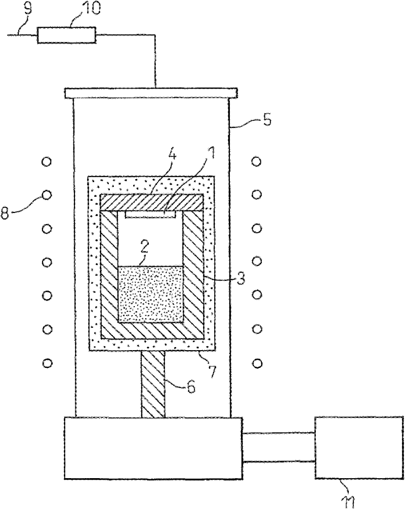
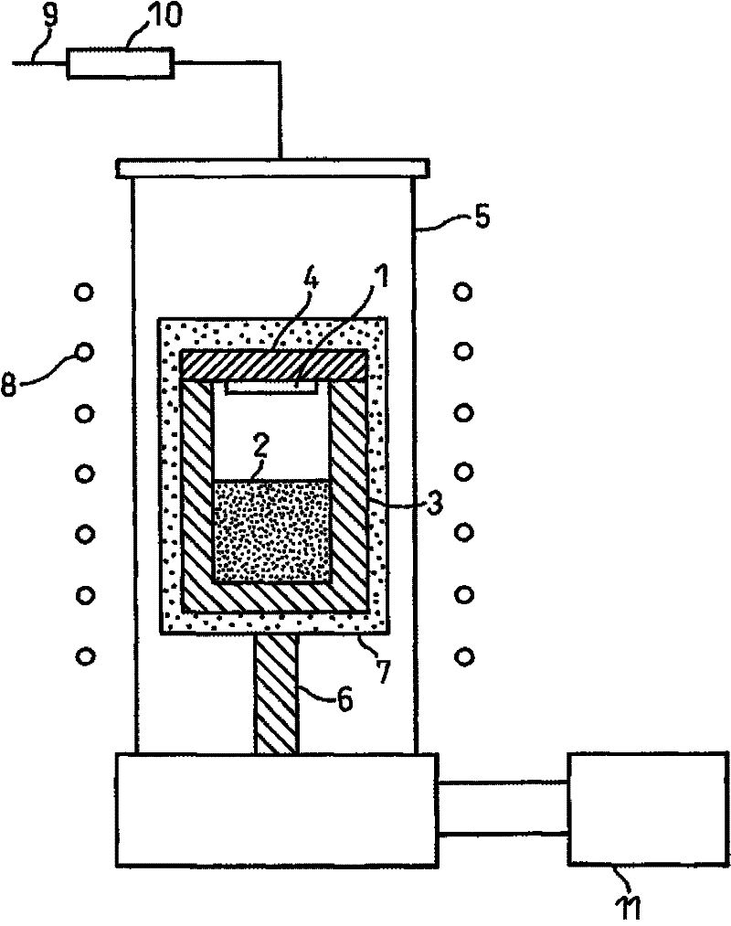
[0063] The nitrogen concentration in the growing crystal is 2.2×10 in the area above 1 mm from the interface with the seed crystal 19 cm -3 Under the conditions of , a SiC single crystal ingot with a diameter of 79 mm was produced by the growth process using the above-mentioned single crystal growth apparatus. In order to make the nitrogen concentration of the growing crystal a desired value, the nitrogen partial pressure in the atmosphere from the estimated time when the growing crystal reached 1 mm to the end of the growth was controlled at 100 Pa, and the nitrogen partial pressure at the start of the growth was set to take into account the nitrogen content of the seed crystal. Concentration etc. values. Next, the seed crystal obtained in this way was machined with a SiC single crystal ingot to produce a plurality of wafers with a diameter of 77 mm in which the {0001...
Embodiment 2
[0070] In order to make the seed crystal for crystal growth of Example 2 by the growth process using the above-mentioned single crystal growth apparatus, the nitrogen concentration in the grown crystal was 5.1×10 in the region of 2 mm or more from the interface with the seed crystal. 19 cm -3 SiC single crystal ingot with a diameter of 103mm. In this case, the nitrogen partial pressure was controlled at 230 Pa except at the beginning of the growth. This ingot was machined to produce a plurality of 101 mm diameter {0001} plane 8° offset wafers, both sides were ground, and one wafer was observed for etch pits. The densities of etch pits corresponding to threading dislocations and basal dislocations are 6.8×10 3 cm -2 , 1.8×10 3 cm -2 , the total density of the pits caused by various dislocations is 8.6×10 3 cm -2 , the density of pits due to microtubules is 1.1 cm -2 .
[0071] Using one of the remaining wafers as a seed crystal, the SiC single crystal of Example 2 was ...
Embodiment 3
[0078] In the same manner as in Example 1, a SiC single crystal ingot with a diameter of 79 mm was produced and used as a seed crystal. Except at the beginning of growth, the nitrogen partial pressure was controlled at 1 kPa, so that the nitrogen concentration of the growing crystal from the region 1 mm away from the seed crystal was 2.0×10 20 cm -3 .
[0079] This ingot was machined to produce a plurality of {0001} plane 8° offset wafers with a diameter of 77 mm, both surfaces were ground, and one wafer was observed for etch pits. The densities of etch pits corresponding to threading dislocations and basal dislocations are 5.6×10 3 cm -2 , 1.1×10 3 cm -2 , the sum of the pits caused by various dislocations has a density of 6.7×10 3 cm -2 , the density of etch pits originating from microtubules is 0.06 cm-2 .
[0080] Using one of the remaining wafers as a seed crystal, the SiC single crystal of Example 3 was grown by the process using the above-mentioned single crysta...
PUM
| Property | Measurement | Unit |
|---|---|---|
| height | aaaaa | aaaaa |
| height | aaaaa | aaaaa |
| height | aaaaa | aaaaa |
Abstract
Description
Claims
Application Information

