
Semiconductor device

A technology of semiconductors and power semiconductors, which is applied in semiconductor devices, semiconductor/solid-state device components, electric solid-state devices, etc., and can solve the difficulties in miniaturization of power semiconductor chips, low-cost semiconductor devices, and power semiconductor chip manufacturing processes Complicated issues

Inactive Publication Date: 2014-12-03
SANKEN ELECTRIC CO LTD
View PDF8 Cites 0 Cited by
  • Summary
  • Abstract
  • Description
  • Claims
  • Application Information

AI Technical Summary

Problems solved by technology

However, according to this method, the manufacturing process of the power semiconductor chip becomes complicated, or since the above-mentioned structure needs to be additionally provided, it is difficult to realize miniaturization of the power semiconductor chip.
[0011] That is, it is difficult to obtain a semiconductor device with reduced adverse effects of noise and improved reliability at low cost.

Method used


Image

  • Semiconductor device
  • Semiconductor device
  • Semiconductor device

Examples


Embodiment Construction

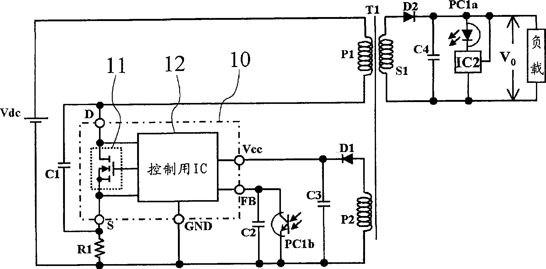
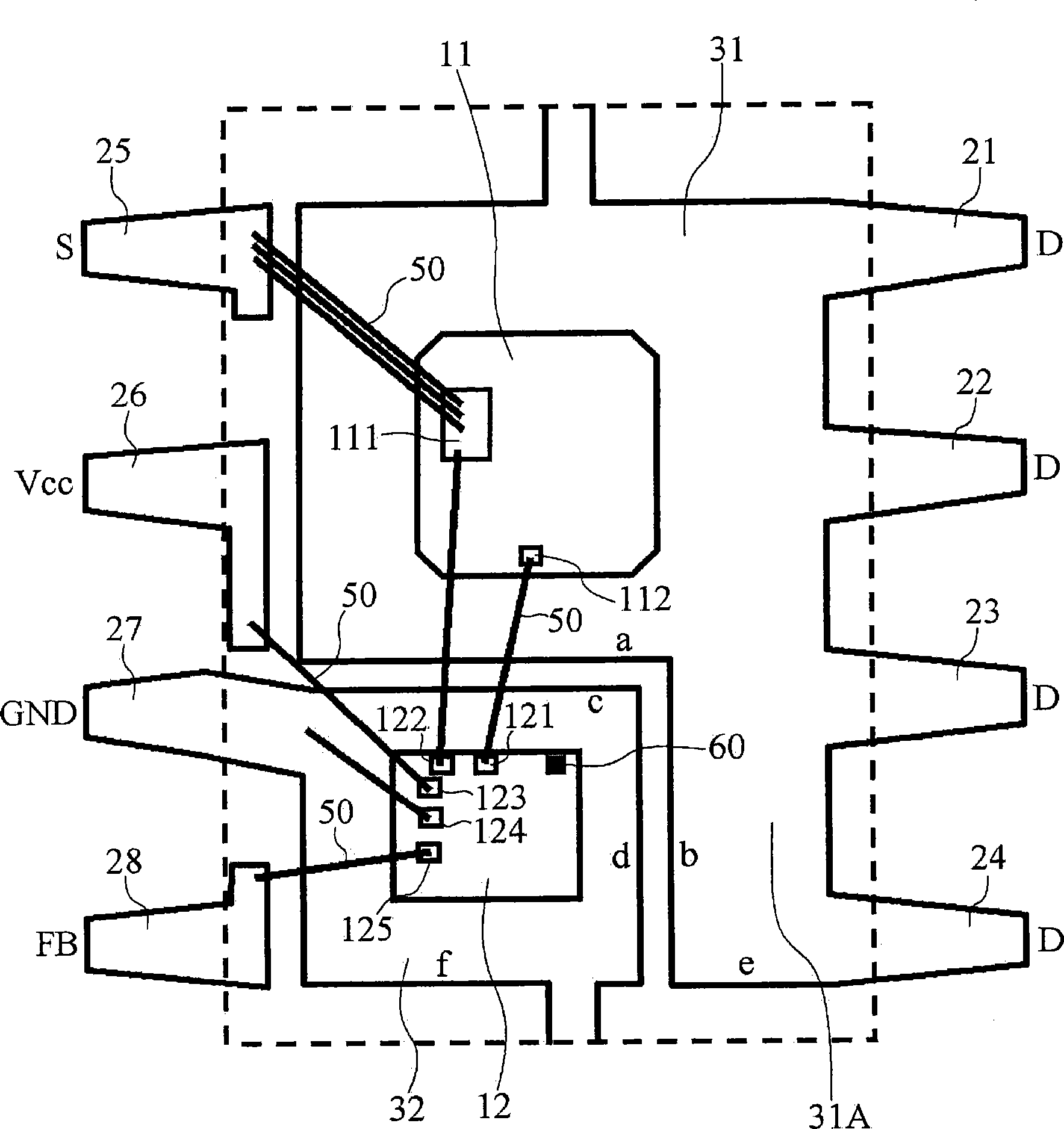
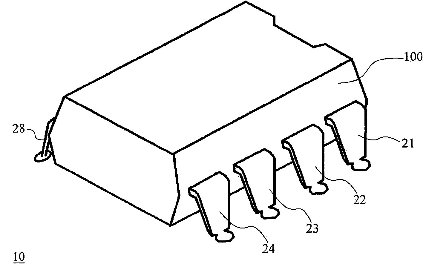
[0020] Next, a power semiconductor module will be described as a semiconductor device according to an embodiment of the present invention. In this semiconductor module package, two semiconductor chips (power semiconductor chip and control IC chip) are respectively mounted on independent heat sinks, and the whole is sealed in a plastic sealing material.

[0021] figure 1 This is an example of a power supply circuit (for example, a standby power supply circuit) realized using the semiconductor module 10 . In this circuit, a region surrounded by a dashed-dotted line corresponds to the semiconductor module 10 including a power semiconductor chip (first semiconductor chip) 11 and a control IC chip (second semiconductor chip) 12 . In this circuit, the output voltage Vo is applied to the load marked on the upper right.

[0022] The power semiconductor chip (first semiconductor chip) 11 is composed of, for example, a rectifying diode, a power-MOSFET, an IGBT (Insulated Gate Bipolar ...


PUM


Abstract

All lead terminals 21 to 24 formed on a first side of a first radiator plate 31 are set as terminals D which are connected to one of the main electrodes of a power semiconductor chip 11 through which a switching current flows. A lead terminal 25 formed on a second side of the first radiator plate 31 is set as a terminal S connected to the other one of the main electrodes of the power semiconductor chip 11. A lead terminal 28 formed on the second side of the first radiator plate 31 is set as a terminal FB to which a control signal of a control IC chip 12 is input. Lead terminals 26 and 27 formed between the lead terminals 25 and 28 are set as a terminal Vcc and a terminal GND, respectively. In this configuration, the potentials at a portion where the lead terminal 26 and a bonding wire 50 connected to the lead terminal 26 exist and at a portion where the lead terminal 27 and a second radiator plate 32 connected to the lead terminal 27 exist are made constant, whereby a noise shield function for suppressing propagation of the switching noise is produced.

Description

technical field [0001] The present invention relates to a semiconductor device having a structure in which two semiconductor chips are built together in a package. Background technique [0002] In a power semiconductor module equipped with a power semiconductor element (rectification diode, power MOSFET, IGBT, etc.) that performs high-current switching or rectification, the power semiconductor element generates a large amount of heat during operation. Therefore, in a power semiconductor module in which a semiconductor chip on which such a power semiconductor element is formed is incorporated in a package, a control IC chip for safely controlling the power semiconductor element is often incorporated together. In such a case, for example, a temperature sensor is mounted on the control IC chip, and control is performed to automatically shut off the power semiconductor element when the heat generation becomes large. Thereby, the safety and reliability of the power semiconductor...

Claims


Application Information

Patent Timeline
Patent Type & Authority Patents(China)
IPC IPC(8): H01L25/16H01L23/48H01L23/34
CPCH01L2224/49112H01L2924/01005H01L2224/48257H01L2224/49111H01L2924/01082H01L2224/48137H01L2924/13091H01L2924/014H01L23/49568H01L23/4952H01L2924/01023H01L24/49H01L2924/01029H01L2224/06051H01L2224/48247H01L2924/01004H01L23/49575H01L2924/3025H01L2924/01006H01L2924/01033H01L2224/0603H01L2924/19041H01L2924/13055H01L24/48H01L2924/1305H01L2924/00014H01L2924/181H01L2924/14H01L2924/00H01L2924/00012H01L2224/45099H01L2224/05599
Inventor 志贺利贵
Owner SANKEN ELECTRIC CO LTD
Features
  • Generate Ideas
  • Intellectual Property
  • Life Sciences
  • Materials
  • Tech Scout
  • Unparalleled Data Quality
  • Higher Quality Content
  • 60% Fewer Hallucinations
Learn More