3D semiconductor memory device and manufacturing method thereof

a semiconductor memory and semiconductor technology, applied in the field of microelectronic technology, can solve the problems of low write-in speed, difficult and the difficulty of conventional flash technology to meet the requirements of memory technology

Active Publication Date: 2012-06-28
INST OF MICROELECTRONICS CHINESE ACAD OF SCI
View PDF26 Cites 81 Cited by
  • Summary
  • Abstract
  • Description
  • Claims
  • Application Information

AI Technical Summary

Benefits of technology

[0009]To overcome the above drawback in the prior art, the present disclosure provides a 3D semiconductor memory device and a manufacturing method thereof, so that a transistor with a smaller size may have a on / off ratio as large as possible.

Problems solved by technology

As a semiconductor device is scaled down, the conventional FLASH technology encounters much severer technical difficulties such as crosstalk, low write-in speed etc.
It is difficult to meet the requirement of the memory technology at 20 nm technology node and beyond.
For example, it is difficult to perform etching on a multilayer structure.
Performances of previously-formed memory cells may be affected when forming subsequent memory cells, which is disadvantageous for high reliable operation of the memory device.
Therefore, the conventional 3D structure must seek tradeoff between the density and performances, which is not a good solution.
The inventor recognized that the prior approaches in the 3D semiconductor memory device had the drawback that the transistor could not have a large on / off ratio while having a reduced layout size of the transistor.

Method used


Image

  • 3D semiconductor memory device and manufacturing method thereof
  • 3D semiconductor memory device and manufacturing method thereof
  • 3D semiconductor memory device and manufacturing method thereof

Examples


Embodiment Construction

[0047]The disclosure will be further illustrated in detail in the following embodiments in conjunction with the accompanying drawings, so that the object, solution and advantages of the present disclosure are more apparent.

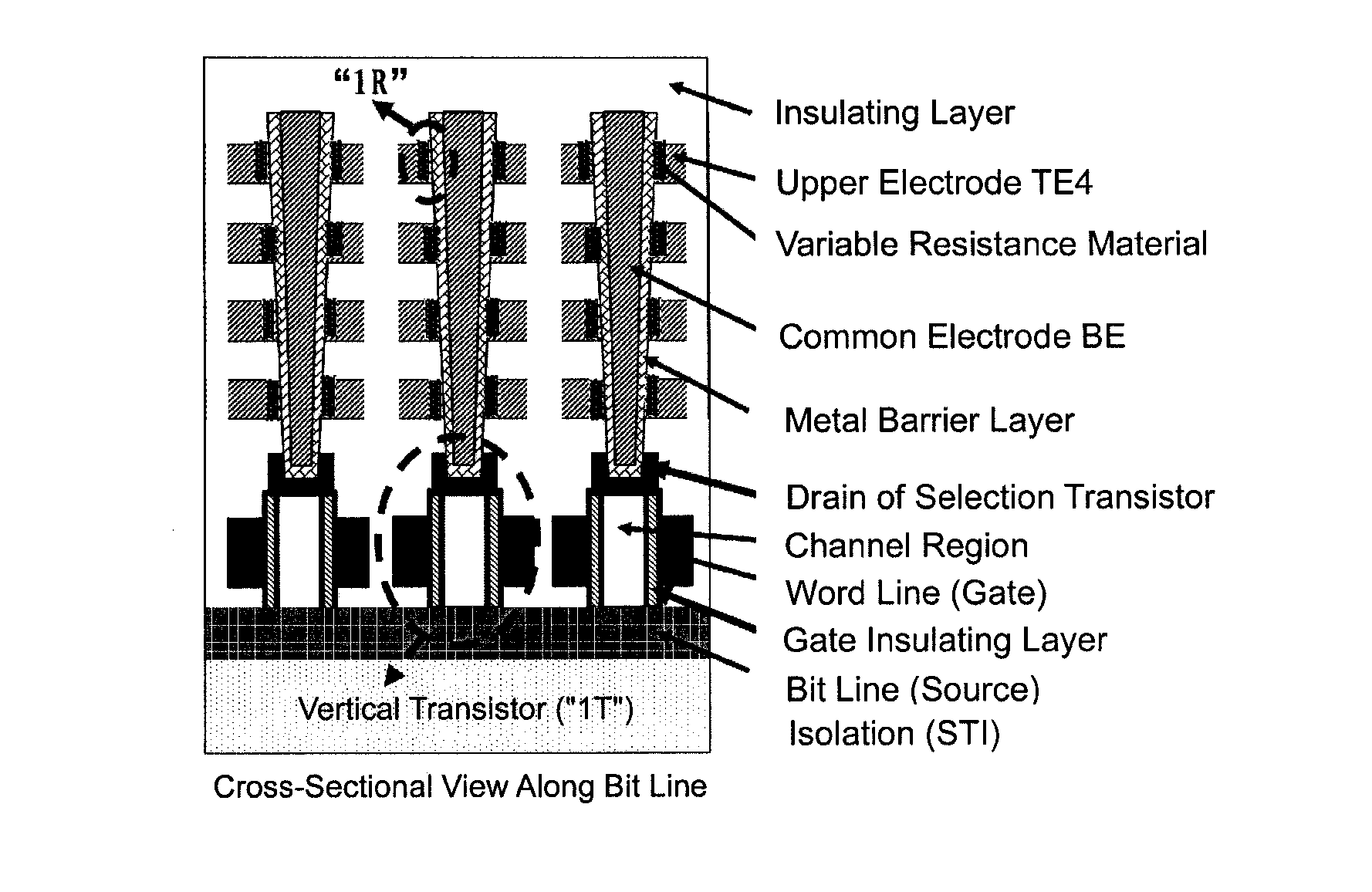
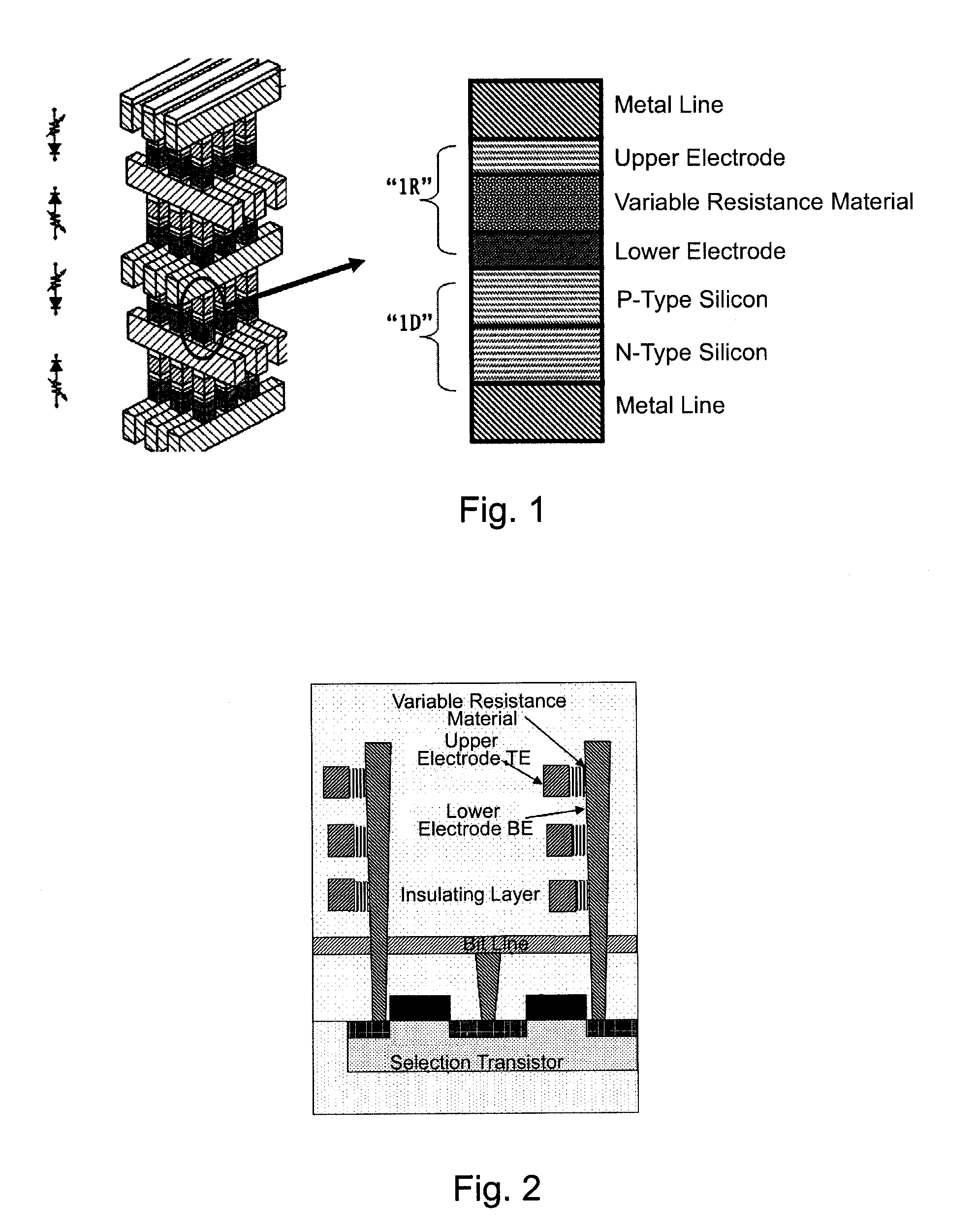
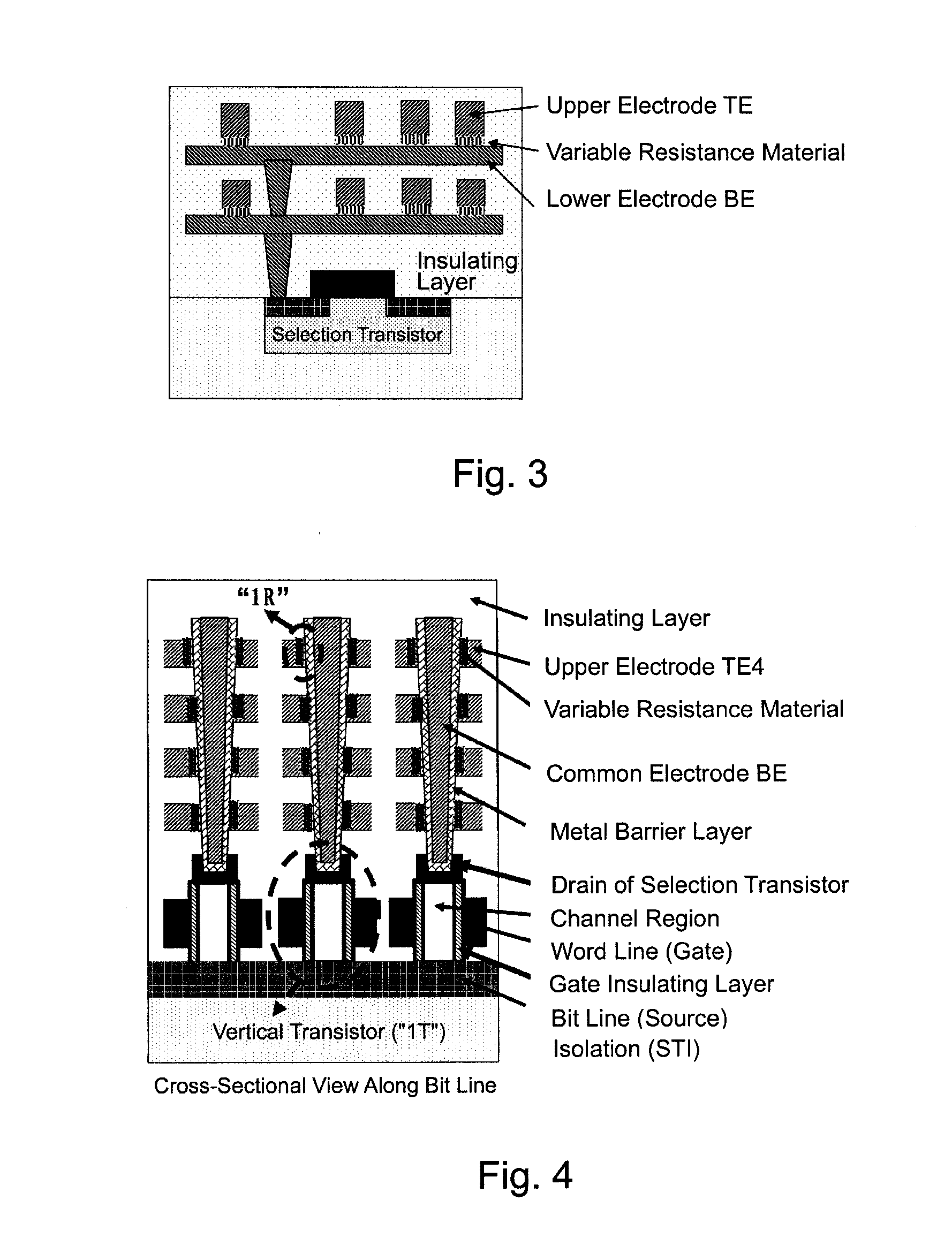
[0048]The present disclosure discloses a 3D semiconductor memory device, comprising; a substrate, and a memory array consisting of one or more of memory cells located on the substrate, each string of memory cells comprising a vertical-type gate-around transistor and a vertical annular variable resistance unit, wherein in a bit line direction, the vertical-type gate-around transistors of the adjacent vertical strings of memory cells have a common source region, gates of the vertical-type gate-around transistors are isolated by an insulating layer, and upper electrodes of the vertical annular variable resistance units are isolated by the insulating layer, the common source region functioning as the bit line of the strings of memory cells; in a word line direction, t...


PUM


Abstract

The present application discloses a 3D semiconductor memory device having 1T1R memory configuration based on a vertical-type gate-around transistor, and a manufacturing method thereof. A on / off current ratio can be well controlled by changing a width and a length of a channel of the gate-around transistor, so as to facilitate multi-state operation of the 1T1R memory cell. Moreover, the vertical transistor has a smaller layout size than a horizontal transistor, so as to reduce the layout size effectively. Thus, the 3D semiconductor memory device can be integrated into an array with a high density.

Description

TECHNICAL FIELD[0001]The present invention relates to microelectronic technology, and more particularly, to a non-volatile high-density 3D semiconductor memory device and a manufacturing method thereof.BACKGROUND[0002]The Semiconductor memory technology is a key one in the microelectronic technology. With the information technology's focus changing from network and computation to storage, researches on the memory technology are becoming a critical research direction in the information technology. Current researches on the memory technology mainly focus on a high-density, high-performance non-volatile FLASH. As a semiconductor device is scaled down, the conventional FLASH technology encounters much severer technical difficulties such as crosstalk, low write-in speed etc. It is difficult to meet the requirement of the memory technology at 20 nm technology node and beyond. Therefore, it is desirable to develop new memory technology to meet mass storage requirements.[0003]Recently, a va...

Claims


Application Information

Patent Timeline
Patent Type & Authority Applications(United States)
IPC IPC(8): H01L45/00H01L21/8239
CPCH01L27/249H01L45/04H01L45/06H01L27/2454H01L45/144H01L45/146H01L45/147H01L45/1226H10B63/34H10B63/845H10N70/823H10N70/231H10N70/20H10N70/8836H10N70/8828H10N70/8833
Inventor HUO, ZONGLIANGLIU, MING
Owner INST OF MICROELECTRONICS CHINESE ACAD OF SCI
Why Eureka
Try Eureka