Magnetic memory element and storage device using the same

a memory element and memory technology, applied in the field of magnetic memory elements, can solve the problems of high writing energy, low capacity mram is not suitable for replacing the dram technique, and large cell area, and achieve the effects of reducing the magnetic anisotropic energy, high thermal stability, and reducing the current required for writing

Active Publication Date: 2012-03-29
III HLDG 3
View PDF2 Cites 82 Cited by
  • Summary
  • Abstract
  • Description
  • Claims
  • Application Information

AI Technical Summary

Benefits of technology

[0040]According to the magnetic memory element and the storage device of the invention, the internal stress of a magnetic body serving as a storage layer is changed to reduce the magnetic anisotropic energy during writing. As a result, the current required for writing is reduced. During the pe

Problems solved by technology

The first problem of the MRAM is a large cell area and high writing energy.
Ther

Method used


Image

  • Magnetic memory element and storage device using the same
  • Magnetic memory element and storage device using the same
  • Magnetic memory element and storage device using the same

Examples


first embodiment

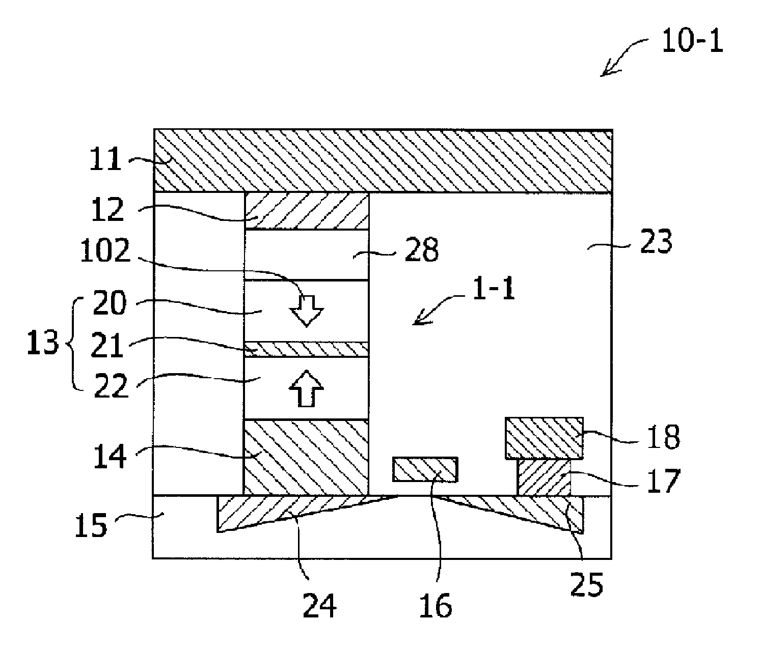
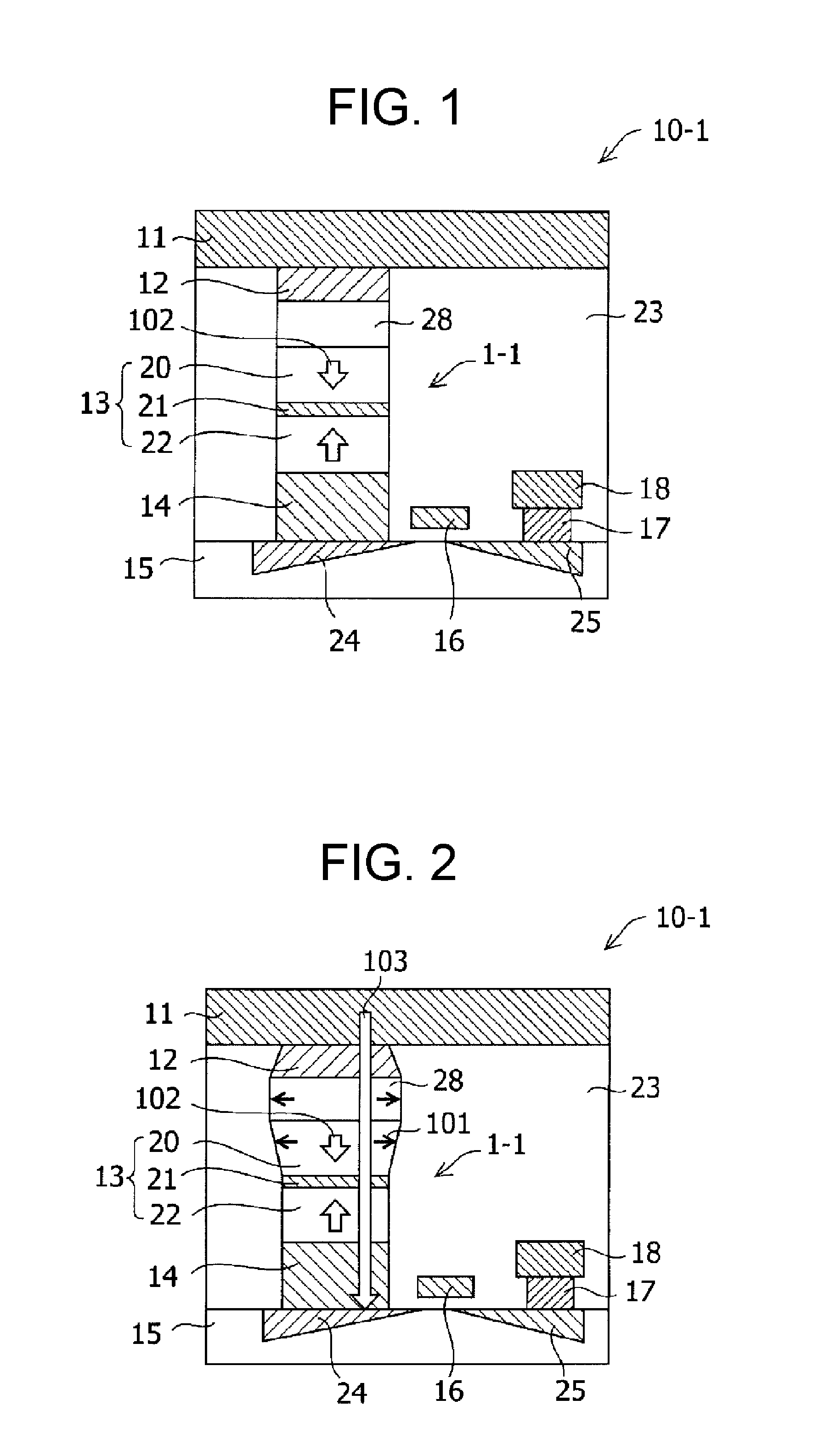
[0064]FIG. 1 is an enlarged cross-sectional view illustrating a portion of a storage device 10-1 including a magnetic memory element 1-1. In FIGS. 1 and 2, the same components as those shown in FIG. 12 are denoted by the same reference numerals and a description thereof will not be repeated. The structure of the magnetic memory element 1-1 according to this embodiment is different from that of the magnetic memory element 1′ according to the related art shown in FIG. 12 in that a thermal expansion layer 28 is inserted between a storage layer 20 and an upper electrode 12. The principle of the reading and writing operations of the magnetic memory element 1-1 is the same as that of the reading and writing operations of the magnetic memory element 1′ according to the related art and thus a description thereof will not be repeated.

[0065]The magnetic memory element 1-1 including the thermal expansion layer 28 can reduce a writing current for the following reason. That is, the writing (STT)...

second embodiment

[0081]FIG. 6 is an enlarged cross-sectional view illustrating a portion of a storage device 10-2 including a magnetic memory element 1-2 according to a second embodiment. In FIG. 6, the same components as those shown in FIG. 1 are denoted by the same reference numerals and a description thereof will not be repeated.

[0082]The magnetic memory element 1-2 according to this embodiment uses in-plane magnetization films that are magnetized in the left-right direction in FIG. 6 as the storage layer 20 (second magnetic body) and the pinned layer 22 (first magnetic body). In addition, the magnetic memory element 1-2 includes a thermal contraction layer 29 instead of the thermal expansion layer 28 shown in FIG. 1.

[0083]As described above, the magnetic memory element 1-1 according to the first embodiment shown in FIG. 1 is strained by the thermal expansion layer 28 in the direction in which the cross-sectional area (a cross section parallel to the interface between the storage layer 20 and the...

third embodiment

[0089]FIG. 7 is an enlarged cross-sectional view illustrating a portion of a storage device 10-3 including a magnetic memory element 1-3 according to a third embodiment. In FIG. 7, the same components as those shown in FIG. 1 are denoted by the same reference numerals and a description thereof will not be repeated.

[0090]The structure of the magnetic memory element 1-3 according to this embodiment is different from that of the magnetic memory element 1-1 according to the first embodiment shown in FIG. 1 in that an expansion and contraction layer 30 is provided between the interlayer insulating film 23 and the thermal expansion layer 28. However, in this embodiment, the expansion and contraction layer 30 is also provided between the interlayer insulating film 23 and the storage layer 20.

[0091]In the magnetic memory element 1-1 according to the first embodiment, the thermal expansion layer 28 is thermally expanded by Joule heat generated due to a writing current. At that time, the ther...


PUM


Abstract

A magnetic memory element capable of maintaining high thermal stability (retention characteristics) while reducing a writing current. The magnetic memory element includes a magnetic tunnel junction having a first magnetic body including a perpendicular magnetization film, an insulating layer, and a second magnetic body serving as a storage layer including a perpendicular magnetization film, which are sequentially stacked. A thermal expansion layer is disposed in contact with the magnetic tunnel junction portion. The second magnetic body is deformed in a direction in which the cross section thereof increases or decreases by the thermal expansion or contraction of the thermal expansion layer due to the flow of a current, thereby reducing a switching current threshold value required to change the magnetization direction.

Description

TECHNICAL FIELD[0001]The present invention relates to a magnetic memory element for reading data using a magnetoresistive effect and a nonvolatile storage device using the magnetic memory element.BACKGROUND ART[0002]In recent years, the capacity of a nonvolatile semiconductor storage device whose representative example is a flash memory has increased significantly and a product with a capacity of several hundreds of gigabytes has been released. The nonvolatile semiconductor storage device has a high commercial value as, particularly, a USB memory or a storage device for a mobile phone and is useful as a storage device for a portable music player since it has the advantages of a solid-state element memory, such as vibration resistance, high reliability, and low power consumption. Therefore, the nonvolatile semiconductor storage device has been mainly used as a storage device for a portable or mobile electronic apparatus for music and images.[0003]In addition to the application of the...

Claims


Application Information

Patent Timeline
IPC IPC(8): G11C11/16H01L29/82
CPCB82Y25/00G11C11/16H01F10/3254H01F10/3286B82Y40/00H01L27/228H01L43/08G11C11/161H01F41/303G11C11/1675H10B61/22H10N50/10H10N50/01
Inventor YAMADA, MICHIYAOGIMOTO, YASUSHI
Owner III HLDG 3
Why Eureka
Try Eureka