Trench insulated gate bipolar transistor and manufacturing method thereof

A bipolar transistor, insulated gate technology, applied in the manufacture of semiconductor/solid-state devices, semiconductor devices, electrical components, etc., can solve the problem of increasing the saturation voltage between the collector and the emitter, and improve the contact performance and reduce the contact resistance. Effect

Inactive Publication Date: 2011-09-28
FORCE MOS TECH CO LTD
View PDF5 Cites 21 Cited by
  • Summary
  • Abstract
  • Description
  • Claims
  • Application Information

AI Technical Summary

Problems solved by technology

The trench IGBT device disclosed by Huang et al. also has its own shortcomings, because the depth of the P+ base region 35 is greater than the depth of the P-type base region 14, causing a gap between two adjacent contact trenches. Has a higher JFET resistance, and an increase in the JFET resistance will cause an increase in the collector-emitter saturation voltage

Method used


Image

  • Trench insulated gate bipolar transistor and manufacturing method thereof
  • Trench insulated gate bipolar transistor and manufacturing method thereof
  • Trench insulated gate bipolar transistor and manufacturing method thereof

Examples


Embodiment Construction

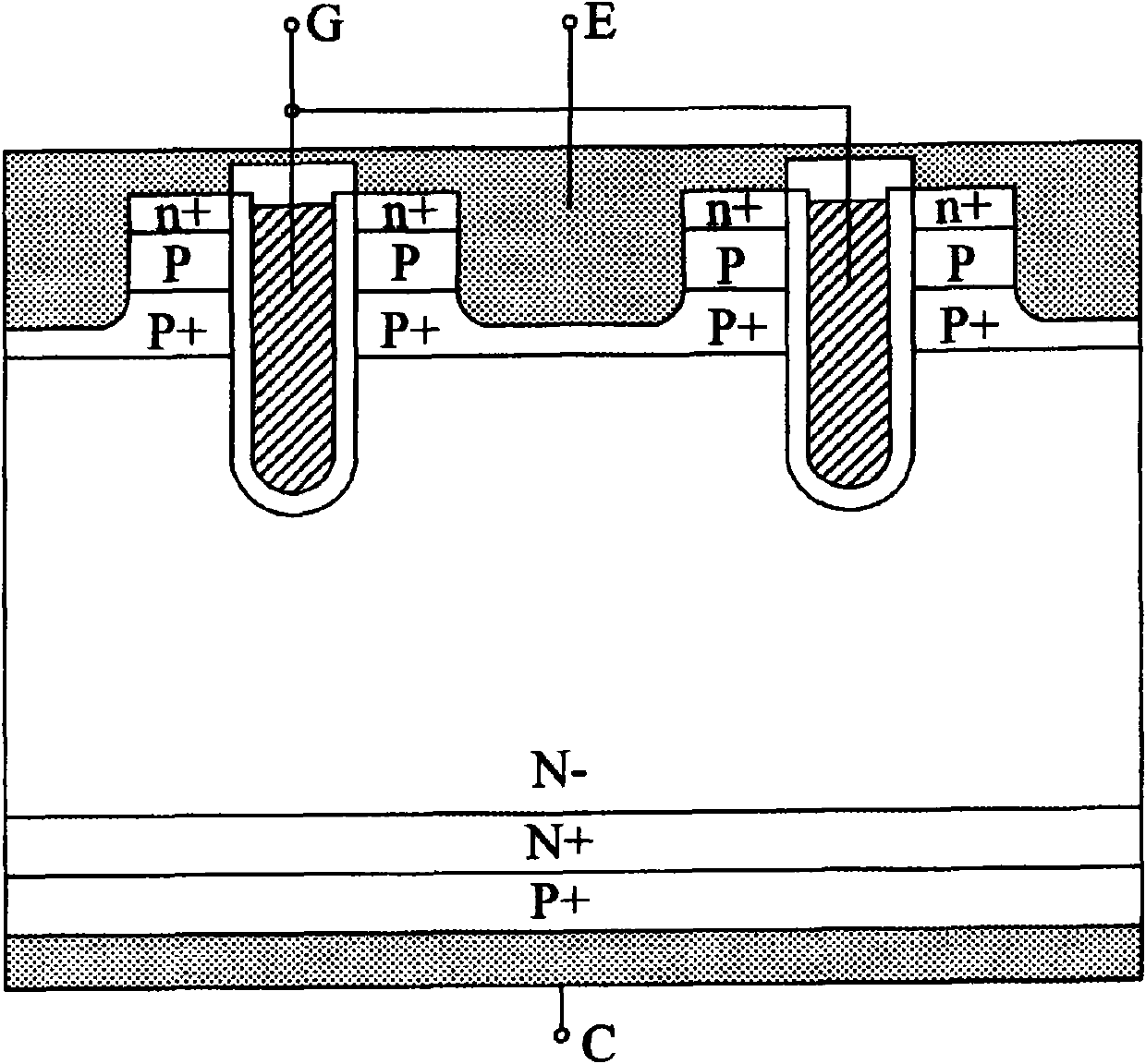
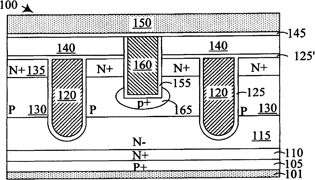
[0041] Figure 2A A cross-sectional view of a trench insulated gate bipolar transistor (IGBT) device 100 , which is a vertical power device formed on a P+ substrate 105 , according to an embodiment of the present invention is shown. see Figure 2A , the trench IGBT device is a punch-through (PT) device. The P+ substrate 105 is used as a collector region, and a collector metal 101 is formed on its lower surface. On the upper surface of the P+ substrate 105, an N+ epitaxial layer 110 and an N− epitaxial layer 115 are grown in sequence. The trench IGBT device further includes a trench gate 120 , the inner surface of the trench gate 120 is lined with a gate oxide layer 125 and filled with polysilicon. The trench gate 120 is surrounded by a P-type base region 130 , and includes an N+ emitter 135 near the upper surface of the P-type base region 130 . The insulating layer 140 covers the upper surface of the substrate and covers the insulating layer 125' formed simultaneously with...


PUM


Abstract

The invention discloses a trench insulated gate bipolar transistor (IGBT) device. According to the invention, an emitter region-base region contact doping zone with a P<+> type is included. The doping zone is in a P-type base and at least encompasses the lowest part of an emitter region-base region contact trench. The concentration of the majority carriers in the emitter region-base region contact doping zone is higher than that of the P-type base, and the emitter region-base region contact doping zone keeps a predetermined distance from a channel region nearby trench gates, so that it can be guaranteed that an emitter electrode-base electrode resistor can be reduced under the condition that a grid electrode- emitter electrode threshold voltage is not improved.

Description

technical field [0001] The invention relates to a device structure and a manufacturing method of an insulated gate bipolar transistor (IGBT). In particular, it relates to a device structure and a manufacturing method of a trench IGBT with improved emitter-base contact characteristics and metal wiring. Background technique [0002] As a widely used power electronic device, semiconductor power devices are used in power electronic systems such as hybrid, electric or fuel cell locomotives. In recent years, the market demand for high-performance semiconductor power devices is increasing, especially for high-voltage semiconductor power devices such as IGBTs. However, traditional high-voltage semiconductor power devices such as IGBTs still face technical difficulties due to the increase of the saturation voltage between the collector and emitter. Especially when the manufacture of IGBTs is becoming more and more miniaturized and the unit density of semiconductor power devices is ...

Claims


Application Information

Patent Timeline
Patent Type & Authority Applications(China)
IPC IPC(8): H01L29/739H01L29/06H01L21/331
Inventor 谢福渊
Owner FORCE MOS TECH CO LTD
Why Eureka
Try Eureka