
silicon controlled rectifier

A silicon-controlled rectifier and silicided metal technology, applied in semiconductor devices, electrical components, diodes, etc., can solve the problem of reducing parasitic transistor pairs or silicon-controlled rectifier SCR opening speed, parasitic PNP and NPN transistor amplification factor reduction, large time constant, etc. problem, to achieve the effect of improving ESD protection capability, increasing opening speed, and increasing amplification factor

Active Publication Date: 2016-01-06
SHANGHAI HUAHONG GRACE SEMICON MFG CORP
View PDF4 Cites 0 Cited by
  • Summary
  • Abstract
  • Description
  • Claims
  • Application Information

AI Technical Summary

Problems solved by technology

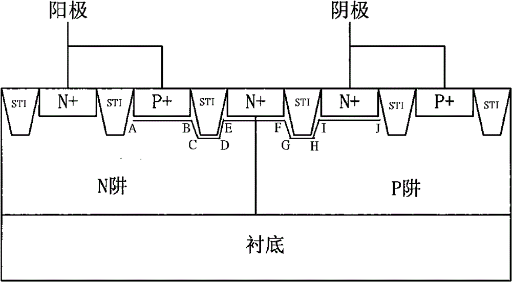
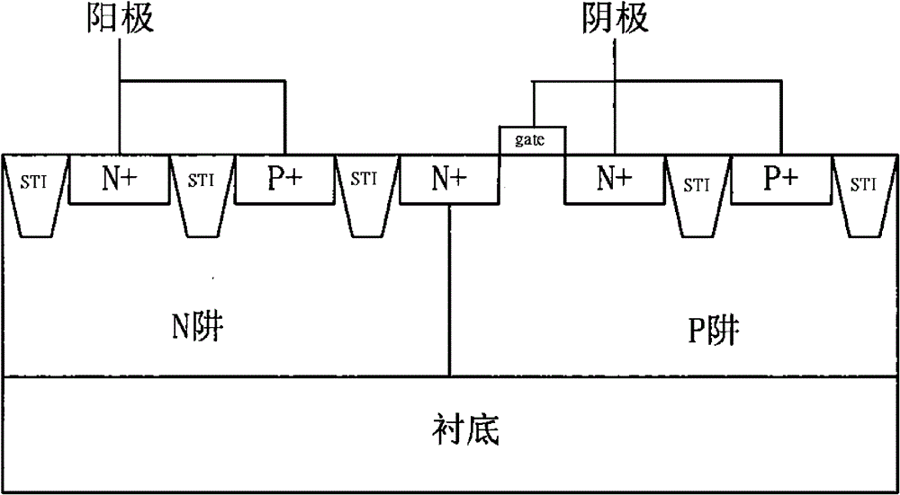
[0005] However, the structure of the above-mentioned silicon controlled rectifier has the following disadvantages: due to the existence of shallow trench isolation (STI) between NP junctions in the PNPN structure, the SCR trigger current path is relatively long. Taking MLSCR as an example, as figure 1 As shown, the trigger current path needs to go through A-B-C-D-E-F-G-H-I-J, which will cause its parasitic resistance R and parasitic capacitance C to be relatively large, and the amplification factor β of the parasitic PNP and NPN transistor formed by its PNPN structure is reduced. On the other hand, due to the parasitic resistance R And the birth capacitor C will cause the time constant τ=RC to be larger and further reduce the opening speed of the parasitic triode pair or the silicon controlled rectifier SCR. In other words, when a narrow pulse with a higher frequency or a shorter duration comes, the current The ESD protection circuit of the PNPN structure described in the prior art cannot play its due protection function in time, that is, the STI of the NP junction affects the normal protection function of ESD
[0006] To sum up, it can be known that the silicon controlled rectifiers of the prior art have the problem that the shallow trench isolation structure (STI) affects the normal protection function of ESD electrostatic discharge, so it is necessary to propose improved technical means to solve this problem

Method used


Image

  • silicon controlled rectifier
  • silicon controlled rectifier
  • silicon controlled rectifier

Examples


Embodiment Construction

[0025] The implementation of the present invention is described below through specific examples and in conjunction with the accompanying drawings, and those skilled in the art can easily understand other advantages and effects of the present invention from the content disclosed in this specification. The present invention can also be implemented or applied through other different specific examples, and various modifications and changes can be made to the details in this specification based on different viewpoints and applications without departing from the spirit of the present invention.

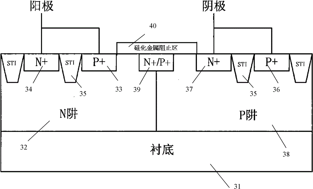
[0026] image 3 It is a sectional view of the SCR structure of a preferred embodiment of the present invention. In this preferred embodiment, the ESD protection circuit is MLSCR, such as image 3 As shown, a silicon controlled rectifier of the present invention includes: a semiconductor substrate 31, which can be a P substrate or an N substrate; a well region is formed on the substrate 31,...


PUM


Abstract

The invention discloses a silicon controlled rectifier which comprises a semiconductor substrate; an N well and a P well formed above the semiconductor substrate; a first P+ doped zone and a first N+ doped zone formed in the N well; a second P+ doped zone and a second N+ doped zone formed in the P well; a third doped zone formed in the joint position of the N well and the P well; and a salicide block zone formed above the third doped zone. According to the invention, by using the salicide block zone, current path is diminished, the amplifier coefficient of parasitic triode formed by the PNPN structure is increased, thereby the starting speed of the silicon controlled rectifier is increased, and the ESD protection capability of the silicon controlled rectifier is improved.

Description

technical field [0001] The present invention relates to a semiconductor device, in particular to a silicon controlled rectifier. Background technique [0002] With the increasingly advanced semiconductor process, more and more designers pay more and more attention to the protection of electrostatic discharge (ESD) in IC design. The components that make up the ESD protection circuit include resistors (Resistor), diodes (Diode), triodes (Bipolar), gate grounded metal oxide half field effect transistors (GGMOSFET), gate coupled metal oxide half field effect transistors (GCMOSFET), silicon controlled rectifier (SCR), etc. [0003] Among many ESD protection devices, the Silicon Controlled Rectifier (SCR) has the best ESD protection capability under the same area due to its low sustain voltage. However, when the SCR structure is used as an ESD protection device, it has a high trigger voltage value, which makes the ESD protection effect of the entire circuit not as ideal as expec...

Claims


Application Information

Patent Timeline
Patent Type & Authority Patents(China)
IPC IPC(8): H01L29/87H01L29/06
CPCH01L29/87
Inventor 胡剑
Owner SHANGHAI HUAHONG GRACE SEMICON MFG CORP
Learn More