Semiconductor structure with through holes and manufacturing method thereof

A manufacturing method and semiconductor technology, applied in the direction of semiconductor/solid-state device manufacturing, semiconductor devices, semiconductor/solid-state device components, etc., to achieve the effects of improving performance, increasing flexibility, and improving stress

Inactive Publication Date: 2011-10-12
PEKING UNIV
View PDF6 Cites 43 Cited by
  • Summary
  • Abstract
  • Description
  • Claims
  • Application Information

AI Technical Summary

Problems solved by technology

[0005] In view of the above problems, the object of the present invention is to provide a semiconductor structure with through holes, which can not only ensure good power integrity and heat dissipation between stacked chips, but also effectively improve the stress and warpage of the through hole structure And other issues

Method used


Image

  • Semiconductor structure with through holes and manufacturing method thereof
  • Semiconductor structure with through holes and manufacturing method thereof
  • Semiconductor structure with through holes and manufacturing method thereof

Examples


Embodiment 1

[0048]Firstly, the semiconductor structure with through holes provided by the present invention is summarized below. The semiconductor structure includes a substrate 100, a plurality of annular through holes 302, and a plurality of solid through holes 301, wherein:

[0049] The substrate 100 has opposite first surface 100-1 and second surface 100-2;

[0050] The annular through hole 302 and the solid through hole 301 are embedded in the substrate and penetrate through the substrate 100 in a direction perpendicular to the first surface 100-1 and the second surface 100-2;

[0051] The solid through hole 301 is filled with a solid metal plug 340;

[0052] The annular through hole 302 is filled by a solid dielectric plug 350 and a metal ring 330 surrounding the solid dielectric plug.

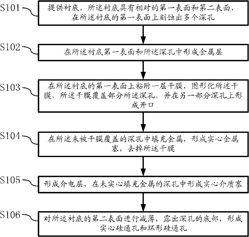
[0053] The semiconductor manufacturing method such as figure 1 shown, including the following steps:

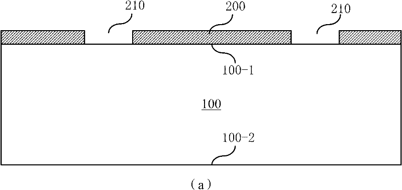
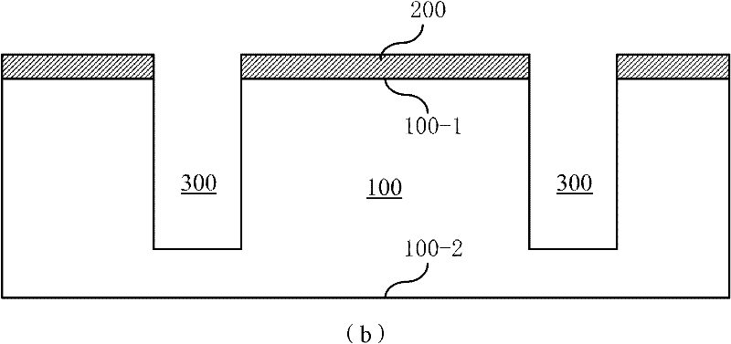
[0054] In step S101, a substrate 100 is provided, the substrate 100 has opposite first surfa...

Embodiment 2

[0064] Optionally, the semiconductor structure with through holes in this embodiment can be based on the semiconductor structure in Embodiment 1, between the metal plug 340 of the solid through hole 301 and the substrate 100, and the metal ring of the annular through hole 302 Between 330 and the substrate 100 , an insulating layer 310 connected to the substrate and a barrier layer 320 surrounding the metal plug 340 and the metal ring 330 are added.

[0065] On the basis of the manufacturing method of embodiment 1, increase following steps:

[0066] After etching the deep hole 300 in step S101, an insulating layer 310 is formed on the first surface 100-1 of the substrate 100 and the deep hole 300;

[0067] After the above-mentioned insulating layer 310 is formed, a barrier layer 320 is formed on the insulating layer 310 . The barrier layer 320 is present in both the first surface 100 - 1 of the substrate 100 and the deep hole 300 .

[0068] After the above two steps are compl...

Embodiment 3

[0075] Optionally, the semiconductor structure with through-silicon vias in this embodiment can be based on Embodiment 1 or 2, on the first surface 100-1 of the substrate 100, the rewiring layer 510, the interlayer dielectric layer 500, and the metal Bump 520.

[0076] Based on the method in embodiment 2, the manufacturing method of the present embodiment is described as follows:

[0077] After step S105 is performed according to the method of Embodiment 2, a redistribution layer (RDL) 510 and metal bumps 520 are formed on the first surface 100 - 1 of the substrate 100 .

[0078] First, the dielectric layer on the first surface 100 - 1 is removed by appropriate methods such as etching, and the metal layer 330 and the barrier layer 320 are patterned to form a rewiring layer electrically connected to the deep hole 300 .

[0079] Subsequently, an interlayer dielectric layer 500 is formed on the first surface 100-1 of the substrate. The material of the interlayer dielectric layer...


PUM


Abstract

The invention discloses a semiconductor structure with through holes and a manufacturing method thereof. The semiconductor structure comprises a substrate, a plurality of annular through holes and a plurality of solid through holes; the annular through holes and the solid through holes are embedded in the substrate; the solid through holes are through holes filled by metal; and the annular through holes are through holes filled by solid dielectric plugs and metal rings surrounding the solid dielectric plugs. The manufacturing method comprises the steps of: (1) etching a plurality of deep holes on a first surface of the substrate; (2) forming a metal layer; (3) attaching a dry film on the first surface of the substrate and patterning the dry film such that the dry film generates openings on one part of deep holes; (4) filling metal in the deep holes with the openings on the dry film, and removing the dry film; (5) filling dielectric in the remaining deep holes to form the solid dielectric plugs; and (6) thinning a second surface of the substrate. The solid through holes of the semiconductor structure disclosed by the invention can be used for the heat radiation of laminated chips to improve the completeness of a power supply; and the annular through holes can be used for solving the problems, such as stress, warping deformation and the like of the through hole structures.

Description

technical field [0001] The invention relates to the field of semiconductor structure manufacturing, in particular to a semiconductor structure with through holes and a manufacturing method thereof. Background technique [0002] The three-dimensional integration technology based on Through Silicon Via (TSV) interconnection can provide vertical electrical signal interconnection, reduce the parasitic parameters of the wiring, improve the working speed of the system, and reduce power consumption. In addition, it can also provide high-density packaging, reduce the area, volume and weight of microelectronic systems, and has broad application prospects in portable devices or fields with strict requirements on area, volume and weight. The manufacturing process of the TSV structure includes TSV etching, TSV sidewall insulation layer deposition, TSV filling, and bump production. The sequence of each process step can be adjusted according to different applications. , forming a variety...

Claims


Application Information

Patent Timeline
Patent Type & Authority Applications(China)
IPC IPC(8): H01L23/48H01L21/768
CPCH01L2224/13
Inventor 孙新马盛林朱韫晖金玉丰缪旻陈兢
Owner PEKING UNIV
Why Eureka
Try Eureka