Liquid crystal panel, manufacturing method thereof and liquid crystal display

A technology for a liquid crystal panel and a manufacturing method, which can be applied to instruments, nonlinear optics, optics, etc., can solve problems such as glue breakage, and achieve the effects of increasing wet area, avoiding glue breakage, and avoiding light leakage.

Inactive Publication Date: 2011-11-09
BEIJING BOE OPTOELECTRONCIS TECH CO LTD
View PDF3 Cites 14 Cited by
  • Summary
  • Abstract
  • Description
  • Claims
  • Application Information

AI Technical Summary

Problems solved by technology

When the wet area of ​​the sealing glue 13 is less than 4500 square microns, the nozzle of the glue coating equipment will cause glue breakage due to too little glue sprayed out.

Method used


Image

  • Liquid crystal panel, manufacturing method thereof and liquid crystal display
  • Liquid crystal panel, manufacturing method thereof and liquid crystal display
  • Liquid crystal panel, manufacturing method thereof and liquid crystal display

Examples


Embodiment Construction

[0025] In order to make the objectives, technical solutions, and advantages of the embodiments of the present invention clearer, the technical solutions in the embodiments of the present invention will be described clearly and completely in conjunction with the accompanying drawings in the embodiments of the present invention. Obviously, the described embodiments It is a part of the embodiments of the present invention, not all the embodiments. Based on the embodiments of the present invention, all other embodiments obtained by those of ordinary skill in the art without creative work shall fall within the protection scope of the present invention.

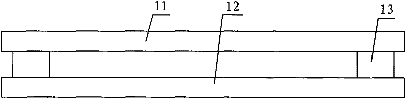
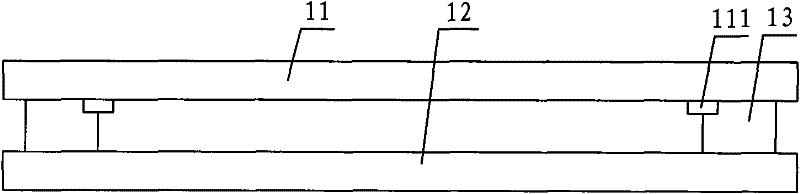
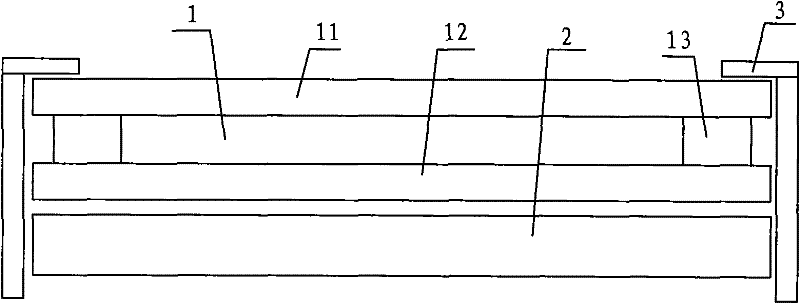
[0026] figure 1 It is a schematic diagram of the structure of a liquid crystal panel provided by the first embodiment of the present invention, such as figure 1 As shown, the liquid crystal panel includes: a color filter substrate 11 and an array substrate 12 arranged in a cell. A frame sealant 13 is formed on the edge of the color ...


PUM


Abstract

The invention discloses a liquid crystal panel, a manufacturing method thereof and a liquid crystal display. The liquid crystal panel comprises a colorful film substrate and an array substrate which are cased, wherein a frame seal adhesive is formed on the edge of the colorful film substrate or the edge of the array substrate, and contains a black light-blocking material. By the liquid crystal panel, the manufacturing method thereof and the liquid crystal display provided by the embodiment of the invention, the frame seal adhesive formed on the edge of the colorful film substrate and the edge of the array substrate contains the black light-blocking material, can block the light emitted by a backlight module to prevent light leakage, and is not required to be formed on a black array, compared with the prior art, the thickness of the frame seal adhesive is increased, the wet area of the frame seal adhesive is improved, and the occurrence of broken adhesive is effectively prevented.

Description

Technical field [0001] The invention relates to liquid crystal display technology, in particular to a liquid crystal panel, a manufacturing method thereof, and a liquid crystal display. Background technique [0002] Liquid crystal displays are currently commonly used flat panel displays, among which ThinFilm Transistor Liquid Crystal Display (TFT-LCD) is the mainstream product in liquid crystal displays. As the thinning and lightness of liquid crystal displays has become the mainstream, increasingly stringent requirements have been placed on the thickness, size and quality of liquid crystal panels in the process of manufacturing liquid crystal displays. [0003] Figure 8 Is a schematic diagram of the structure of a liquid crystal panel in the prior art, such as Figure 8 As shown, the color filter substrate 11 and the array substrate 12 are cell-sealed to form a liquid crystal panel by the frame sealing glue 13, and the frame sealing glue 13 is arranged on the edge of the liquid cry...

Claims


Application Information

Patent Timeline
Patent Type & Authority Applications(China)
IPC IPC(8): G02F1/1339G02F1/1333
Inventor 陈东
Owner BEIJING BOE OPTOELECTRONCIS TECH CO LTD
Why Eureka
Try Eureka