Supercharge Your Innovation With Domain-Expert AI Agents!

Waste heat utilization device for semiconductor production line and operating method thereof

A production line and semiconductor technology, applied in semiconductor/solid-state device manufacturing, electrical components, circuits, etc., can solve problems such as waste and increased production costs, and achieve the effect of reducing manufacturing costs and improving resource utilization

Active Publication Date: 2011-11-16
扬州杰利半导体有限公司
View PDF3 Cites 0 Cited by
  • Summary
  • Abstract
  • Description
  • Claims
  • Application Information

AI Technical Summary

Problems solved by technology

[0002] Most of the current semiconductor production workshops are purification workshops, and the production equipment inside is likely to generate a large amount of high-temperature gas and discharge it. For example, the high-temperature waste heat emitted by waste heat equipment (diffusion furnace, oven, air compressor...) can generally reach 80 ℃ or so, if this high temperature gas is directly discharged into the air, it is a great waste
In general, semiconductor production workshops have relatively high temperature requirements. At present, air conditioners are usually used to adjust the indoor temperature, which will increase production costs.

Method used


Image

  • Waste heat utilization device for semiconductor production line and operating method thereof
  • Waste heat utilization device for semiconductor production line and operating method thereof

Examples


Embodiment Construction

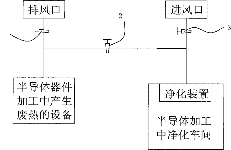
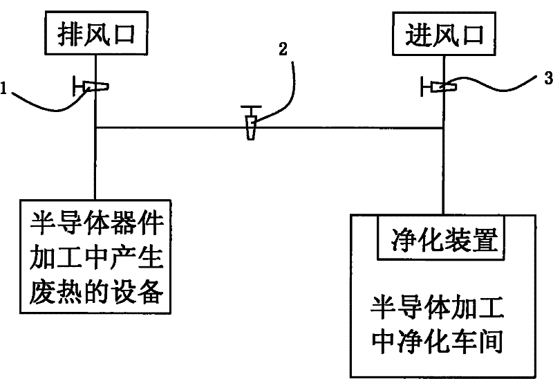
[0014] The invention is like figure 1 As shown, the production line includes equipment that generates waste heat and a purification workshop, which includes an exhaust port, an air inlet, a pipeline, a valve 1, a valve 2, a valve 3, a temperature sensor and a controller, the pipeline Connect the waste heat generating equipment, the purification workshop, the air outlet and the air inlet, the valve one is located at the exhaust outlet, the valve three is located at the air inlet, and the valve two is located at the waste heat generating equipment The temperature sensor includes sensor one, sensor two and sensor three. The first sensor is located at the waste heat outlet of the waste heat generating equipment, and the second sensor is located at the In the purification workshop, sensor three is located outside the air inlet; valves one to three and sensors one to three are connected to the controller respectively.

[0015] The working method of the present invention is:

[0016] 1)...


PUM


Abstract

The invention discloses a waste heat utilization device for a semiconductor production line and an operating method thereof. The invention in particular relates to a heat source recycling device for a purification plant in a semiconductor chip manufactory and the operating method of the device. The device comprises a device for generating waste heat and a purification plant, as well as an air outlet, an air inlet, pipelines, a valve 1, a valve 2 and a valve 3, a temperature sensor and a controller, wherein the device for generating waste heat, the purification plant, the air outlet and the air inlet are connected through the pipelines; the valve 1 is arranged at the position of the air outlet; the valve 3 is arranged at the position of the air inlet; and the valve 2 is arranged on the pipeline between the device for generating waste heat and the purification plant; the temperature sensor comprises a sensor 1, a sensor 2 and a sensor 3; the sensor 1 is arranged at the position of a waste heat outlet of the device for generating waste heat; the sensor 2 is arranged at the position of the purification plant; and the sensor 3 is arranged outside the air inlet; and the valve 1, the valve 2 and the valve 3, as well as the sensor 1, the sensor 2 and the sensor 3, are respectively connected with the controller. Through the recycling of energy sources in a workshop, the resource utilization ratio is improved, the production and manufacturing cost is lowered, and the device and the method are suitable for the production requirements for low carbon and environmentally friendliness.

Description

Technical field [0001] The invention relates to a device for energy recovery and utilization and a working method, and in particular to a device for recycling and utilization of heat sources in a purification workshop of a semiconductor chip manufacturing plant and a working method of the device. Background technique [0002] The current semiconductor production workshops are mostly purification workshops. The production equipment inside is easy to produce a large amount of high-temperature gas and discharge it. For example, the high-temperature waste heat emitted by waste heat equipment (diffusion furnace, oven, air compressor...) can generally reach 80°C. Or so, if this high-temperature gas is directly discharged into the air, it is a great waste. Generally, semiconductor production workshops have relatively high requirements for temperature. At present, air conditioners are usually used to adjust indoor temperature, which will increase production costs. [0003] The contradicti...

Claims


Application Information

Patent Timeline
Patent Type & Authority Applications(China)
IPC IPC(8): H01L21/00
Inventor 汪良恩
Owner 扬州杰利半导体有限公司
Features
  • R&D
  • Intellectual Property
  • Life Sciences
  • Materials
  • Tech Scout
  • Unparalleled Data Quality
  • Higher Quality Content
  • 60% Fewer Hallucinations
Learn More