

Chamber shield for vacuum physical vapor deposition
A vacuum chamber and vapor technology, applied in the field of radio frequency sputtering physical vapor deposition, can solve the problems of film stability and other problems, and achieve the effect of stabilizing the deposition process
- Summary
- Abstract
- Description
- Claims
- Application Information
AI Technical Summary
Problems solved by technology
Method used
Image

Examples
Embodiment Construction
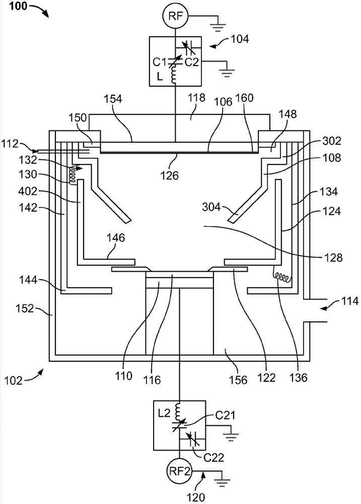
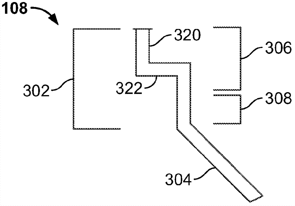
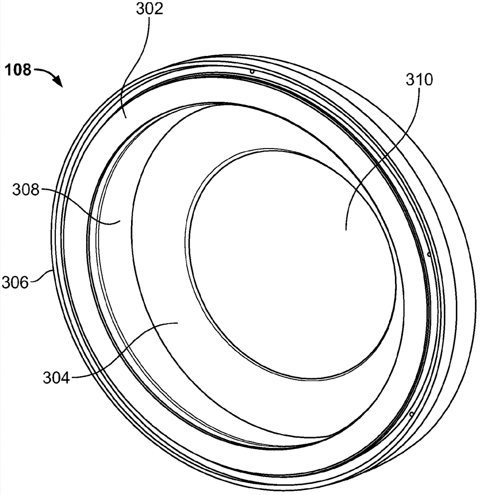
[0022] When RF physical vapor deposition or sputtering is used to form thin films on substrates, there can be variations in plasma density, or plasma can exist in undesired locations within the vacuum chamber, such as between the anode and shield, which can lead to Changes in deposited film properties. By varying the geometry, size and shape of the anode, shield, and electrical connections between the anode and shield, the properties of the deposited film can be controlled.
[0023] refer to figure 1 , the physical vapor deposition apparatus 100 may include a vacuum chamber 102 . The vacuum chamber 102 may be cylindrical and have side walls 152 , a top surface 154 and a bottom surface 156 . Magnetron assembly 118 may be located on top of vacuum chamber 102 . The magnetron assembly 118 may include a set of magnets having alternating poles. The magnetron assembly 118 may be stationary or may rotate about an axis perpendicular to the radius of the vacuum chamber 102 . The ph...
PUM
 Abstract
Description
Claims
Application Information