P-N junction diode structure of MOS (metal-oxide semiconductor)

An oxide semiconductor, P-N technology, applied in the direction of semiconductor devices, transistors, electrical components, etc., can solve the problems of high forward voltage drop and low forward voltage drop, and achieve low forward voltage drop , low leakage current, small reverse bias leakage current effect

Active Publication Date: 2015-05-06
PFC DEVICE
View PDF3 Cites 0 Cited by
  • Summary
  • Abstract
  • Description
  • Claims
  • Application Information

AI Technical Summary

Problems solved by technology

In fact, it is composed of two 300-volt trench Schottky diodes in series, and the forward conduction voltage drop value of the component (V F ) is also higher
How to design components to achieve higher reverse withstand voltage (such as above 600 volts), lower forward conduction voltage drop (V F ), lower reverse leakage current and lower reverse recovery time (Reverse Recovery Time; tRR), that is to say, it has a faster response speed, which is really a big challenge

Method used


Image

  • P-N junction diode structure of MOS (metal-oxide semiconductor)
  • P-N junction diode structure of MOS (metal-oxide semiconductor)
  • P-N junction diode structure of MOS (metal-oxide semiconductor)

Examples


Embodiment Construction

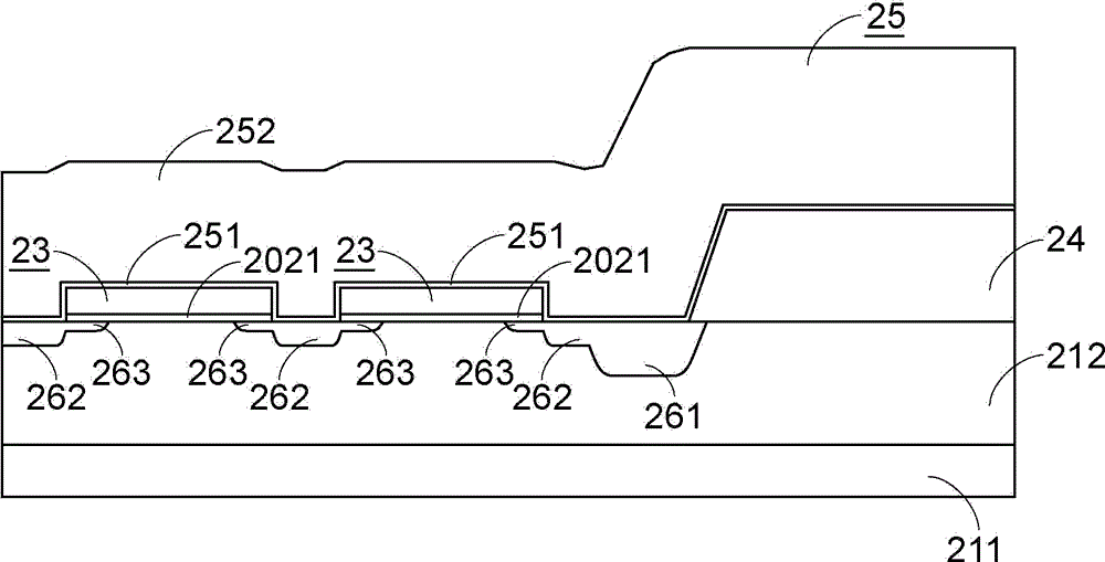
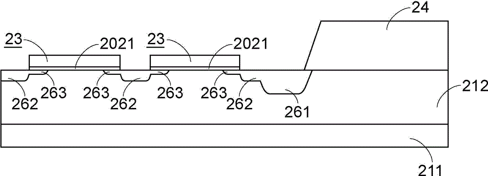
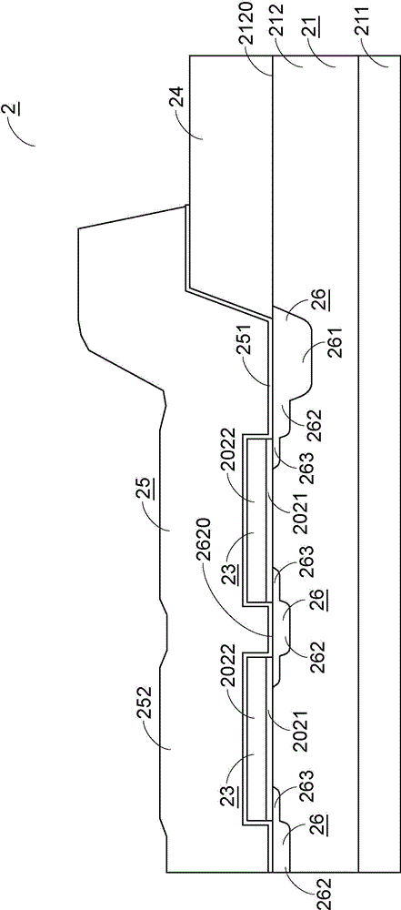
[0033] See Figure 7, which is a schematic diagram of a preferred embodiment of a metal-oxide-semiconductor P-N junction diode structure developed by the present invention to improve the shortcomings of known technical means. From the figure, we can clearly see that the structure of the metal oxide semiconductor P-N junction diode 2 mainly includes a substrate 21, a trench structure 22, a gate structure 23, a sidewall structure 24, a metal layer 25 and an ion implantation region. 26, wherein the substrate 21 is composed of a highly doped N-type silicon substrate (N+ silicon substrate) 211 and a low doped N-type epitaxial layer (N- epitaxial layer) 212, and the trench structure 22 is formed on the substrate 21, the gate structure 23 is formed in the trench structure 22 and protrudes from the surface 2120 of the low-doped N-type epitaxial layer 212, and the sidewall structure 24 protrudes from the surface of the substrate 21 and is located on the gate On the side of the structu...


PUM


Abstract

The invention provides a P-N junction diode structure of an MOS (metal-oxide semiconductor), at least comprising a substrate, a channel structure which is formed above the substrate, a grid electrode structure which is formed in the channel structure and extrudes out of the surface of the channel structure, a side wall structure which extrudes out of the surface of the channel structure and is arranged at one side of the grid electrode structure, a metal layer which is formed on the surface of the channel structure, the surface of the grid electrode structure and the side wall structure, and an ion implantation area of single conductive materials, the ion implantation area is formed on the substrate in a form of multiple regions with different depths and adjacent to the grid electrode structure as well as forms an ohm junction with the metal layer. A diode component has quick response, a positive conduction pressure drop value is low and a back bias voltage leakage current is small.

Description

[0001] The present invention is a divisional application. The filing date of the original application is: April 2, 2009; the original application number is: 200910132565.4; the original invention creation name is: metal oxide semiconductor P-N junction diode structure and its manufacturing method. technical field [0002] The invention relates to a metal oxide semiconductor P-N junction diode structure and a manufacturing method thereof, in particular to a diode with lower leakage current and lower forward conduction voltage drop (V F ), a metal oxide semiconductor P-N junction diode structure with high reverse withstand voltage value and low reverse recovery time characteristics. Background technique [0003] Schottky diode is a unipolar element with electrons as carriers, and its characteristics are fast speed and forward conduction voltage drop value (V F ) is low, but the reverse bias leakage current is relatively large (related to the Schottky barrier value caused by th...

Claims


Application Information

Patent Timeline
Patent Type & Authority Patents(China)
IPC IPC(8): H01L29/06H01L27/082
Inventor 赵国梁郭鸿鑫苏子川
Owner PFC DEVICE
Why Eureka
Try Eureka