Trench vmos transistor manufacturing method

A manufacturing method and transistor technology, which are applied in semiconductor/solid-state device manufacturing, electrical components, circuits, etc., can solve problems such as aluminum puncture, and achieve the effect of increasing the thickness of the metal layer and eliminating the defects of aluminum puncture.

Inactive Publication Date: 2011-11-30
SHANGHAI HUAHONG GRACE SEMICON MFG CORP
View PDF5 Cites 3 Cited by
  • Summary
  • Abstract
  • Description
  • Claims
  • Application Information

AI Technical Summary

Problems solved by technology

[0007] The technical problem solved by the present invention is to provide a method f...

Method used


Image

  • Trench vmos transistor manufacturing method
  • Trench vmos transistor manufacturing method
  • Trench vmos transistor manufacturing method

Examples


Embodiment Construction

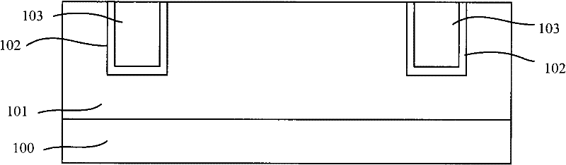
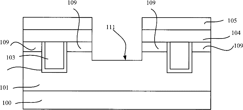
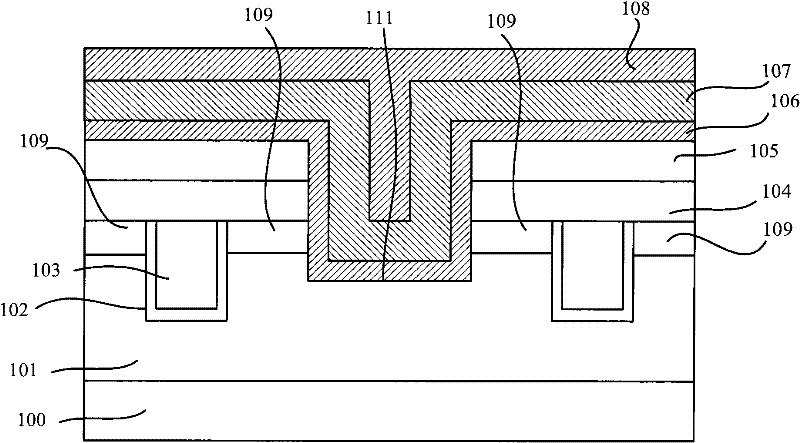
[0028] The inventors have found that the contact holes of existing trench VMOS transistors have relatively large diameters, generally greater than or equal to 0.6 microns, and in some cases up to 2 microns. In the prior art, only chemical vapor deposition or physical vapor deposition is used to form the barrier metal layer on the bottom and sidewall of the trench. Among them, the uniformity of the physical vapor deposition method when depositing the barrier metal layer is not good, so that the formed barrier metal layer is not good at the step of the contact hole, that is, the coverage of the barrier metal layer at the junction of the side wall and the bottom of the contact hole is not good. Well, due to the subsequent high temperature (300-400 degrees Celsius) fabrication of the metal interconnect layer and the metal alloy process, the aluminum of the metal interconnect layer penetrates into the epitaxial layer at the junction of the side wall and the bottom of the contact hol...


PUM

PropertyMeasurementUnit
Thicknessaaaaaaaaaa
Thicknessaaaaaaaaaa

Abstract

The present invention provides a method for manufacturing a trench type VMOS transistor, comprising: providing a semiconductor substrate formed with an epitaxial layer, the epitaxial layer has a trench in it, and a gate is formed in the trench, located on both sides of the gate A source electrode is formed in the epitaxial layer on the side; an interlayer dielectric layer covering the gate is formed above the epitaxial layer, a contact hole is formed in the interlayer dielectric layer and the epitaxial layer, and the contact hole is adjacent to the source electrode ; Forming a metal interconnection layer on the interlayer dielectric layer, and the metal interconnection layer is filled with contact holes; Before the formation of the metal interconnection layer, including the step of: utilizing the method of chemical vapor deposition on the interlayer dielectric The first metal layer is formed on the sidewall and bottom of the contact hole; the second metal layer is formed on the first metal layer by physical vapor deposition, and the second metal layer and the first metal layer constitute the barrier metal layer. The method effectively prevents metal aluminum from entering into the epitaxial layer, and eliminates the defect of aluminum puncture.

Description

technical field [0001] The invention relates to a trench VMOS transistor, in particular to a metallization method for the trench VMOS transistor. Background technique [0002] As the demand for electronic consumer products grows, the demand for power MOSFETs is increasing. Trench Vertical MOS transistors (Trench Vertical MOS) have lower switching loss and higher The fast switching speed is widely used in the field of low voltage power. [0003] In the Chinese patent application with the application number of 200910052544.1, an existing trench VMOS transistor manufacturing method is disclosed. Please refer to Figure 1 ~ Figure 3 . like figure 1 , providing a semiconductor substrate 100, an epitaxial layer 101 is formed on the semiconductor substrate 100, a trench (not marked) is formed in the epitaxial layer 101, and a gate oxide layer 102 is formed on the sidewall and bottom of the trench ; forming a gate 103 filling the trench above the gate oxide layer 102 in the tr...

Claims


Application Information

Patent Timeline
IPC IPC(8): H01L21/336H01L21/768
Inventor 叶康彭树根李乐
Owner SHANGHAI HUAHONG GRACE SEMICON MFG CORP
Why Eureka
Try Eureka