Bipolar thin film transistor and preparation method thereof

A thin film transistor and bipolar technology, which is applied in the field of bipolar thin film transistors and their preparation, can solve the problems of different preparation processes, increased process complexity of CMOS circuits and AM-OLED pixel circuits, and difficulty in obtaining p-type conductance. , to achieve the effect of increasing the complexity of the preparation process and having a great application prospect

Active Publication Date: 2014-12-10
BOE TECH GRP CO LTD
View PDF1 Cites 3 Cited by
  • Summary
  • Abstract
  • Description
  • Claims
  • Application Information

AI Technical Summary

Problems solved by technology

Binary oxides such as ZnO have proven difficult to obtain p-type conductance due to the self-compensation effect
This increases the process complexity of preparing CMOS circuits and AM-OLED pixel circuits: because n-TFT and p-TFT channel materials are different, different preparation processes are required

Method used


Image

  • Bipolar thin film transistor and preparation method thereof
  • Bipolar thin film transistor and preparation method thereof
  • Bipolar thin film transistor and preparation method thereof

Examples


Embodiment Construction

[0015] The present invention will be further described in detail below through specific embodiments in conjunction with the accompanying drawings.

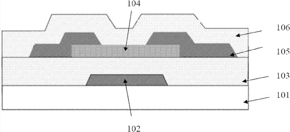
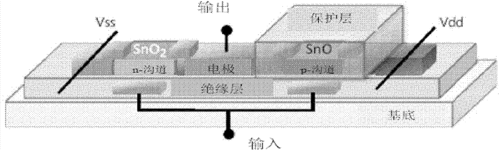
[0016] The present invention proposes a bipolar thin film transistor, such as figure 1 Shown is a schematic structural diagram of the transistor, including: 101 is a substrate; 102 is a gate; 103 is an insulating layer; 104 is an active layer; 105 is a source and drain electrode; 106 is a protective layer. The active layer 104 of the transistor may be:

[0017] Use SnO 2 The thin film is used as the active layer of n-TFT;

[0018] Use SnO or ATO film as the active layer of p-TFT.

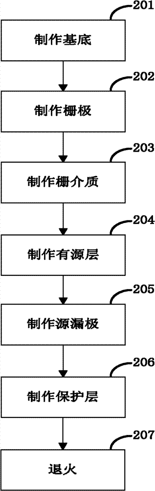
[0019] Such as figure 2 As shown, the preparation method of the above-mentioned bipolar thin film transistor comprises:

[0020] 201. Alkali-free glass as the substrate;

[0021] 202. First prepare a 100nm ITO film by DC magnetron sputtering with an ITO target, and wet etch with dilute hydrochloric acid to form a gate;

[0022] 203. Use SiO agai...


PUM


Abstract

The invention provides a bipolar thin film transistor (TFT). An active layer of the transistor is a SnOx-based thin film. By the bipolar TFT and a preparation method thereof which are provided by the embodiment of the invention, as preparation processes and electric performance of channel materials of a p-TFT and an n-TFT are close to each other, the complexity of the preparation processes of a complementary metal oxide semiconductor (CMOS) circuit (using a SnO or Al-doped SnO2(ATO)p-TFT and a SnO2n-TFT) and an active-matrix organic light emitting diode (AM-OLED) display pixel circuit (in which the SnO2n-TFT is used as a switch TFT and the SnO or ATOp-TFT is used as a driving TFT) can be reduced greatly and the circuit performance can be enhanced; therefore, the bipolar TFT has a great application prospect.

Description

technical field [0001] The invention relates to a bipolar thin film transistor and a preparation method thereof. Background technique [0002] Over the past 30 years, TFT-based large-scale (area) microelectronics technology has led to active matrix liquid crystal display (Active matrix Liquid crystal display, AM-LCD), active matrix light emitting diode display (Active matrix organic light emitting diode, AM-OLED ) and other active matrix flat panel display (Active Matrix Flat Panel Display, AM-FPD) technology rapid development. AM-FPD has become the mainstream technology of modern information display. Currently commercialized AM-FPDs use amorphous silicon thin film transistors (a-Si TFT) or polysilicon thin film transistors (p-Si TFT). In recent years, studies have shown that metal oxide semiconductors (Oxide Semiconductor, OS) have high mobility (10-70cm 2 (V.s) -1 ), optical transparency and low-temperature preparation, and is expected to become a new generation of mai...

Claims


Application Information

Patent Timeline
Patent Type & Authority Patents(China)
IPC IPC(8): H01L29/786H01L21/336
Inventor 姚建可张盛东
Owner BOE TECH GRP CO LTD
Why Eureka
Try Eureka