
Rolled copper foil or electrolytic copper foil for electronic circuits and method of forming electronic circuits using them

A technology of electronic circuit and rolling copper foil, which is applied in the direction of chemical/electrolytic method to remove conductive material, printed circuit, printed circuit, etc., to achieve the effect of shortening time, reducing thickness, and excellent electronic circuit forming method

Inactive Publication Date: 2011-11-30
JX NIPPON MINING & METALS CORP
View PDF11 Cites 5 Cited by
  • Summary
  • Abstract
  • Description
  • Claims
  • Application Information

AI Technical Summary

Problems solved by technology

These problems are: after the circuit is formed, the resin needs to be removed, and the metal or alloy layer with a low etching rate for preventing "bending" needs to be removed by soft etching; Copper foil with a metal or alloy layer (nickel or nickel alloy layer) is used as a copper clad laminate to form an electronic circuit, and copper foil needs to be treated at high temperature in processes such as resin bonding
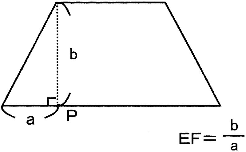
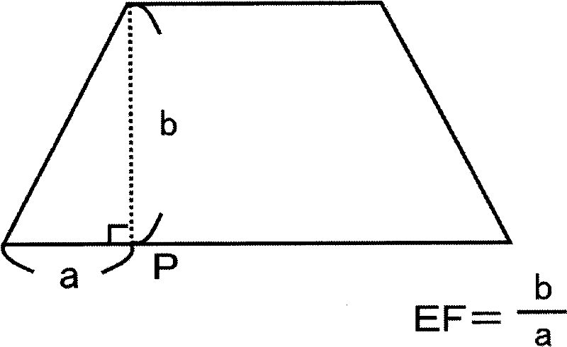
[0018] However, these technologies are not proposed for the purpose of preventing or suppressing the etching of the etched part of the copper foil from the surface of the copper foil downward and widening the end of the copper foil (generating downward bending) when designing the copper foil circuit based on etching. , so the above problem cannot be solved

Method used


Image

  • Rolled copper foil or electrolytic copper foil for electronic circuits and method of forming electronic circuits using them
  • Rolled copper foil or electrolytic copper foil for electronic circuits and method of forming electronic circuits using them
  • Rolled copper foil or electrolytic copper foil for electronic circuits and method of forming electronic circuits using them

Examples


Embodiment 1

[0195] Electrodeposited copper foil of 5 μm is used. The surface roughness Rz of this electrolytic copper foil was 3 micrometers. Under the above-mentioned nickel-zinc alloy plating condition (1), 390 μg / dm is formed on the glossy (S) surface of the electrolytic copper foil 2 nickel-zinc alloy coating.

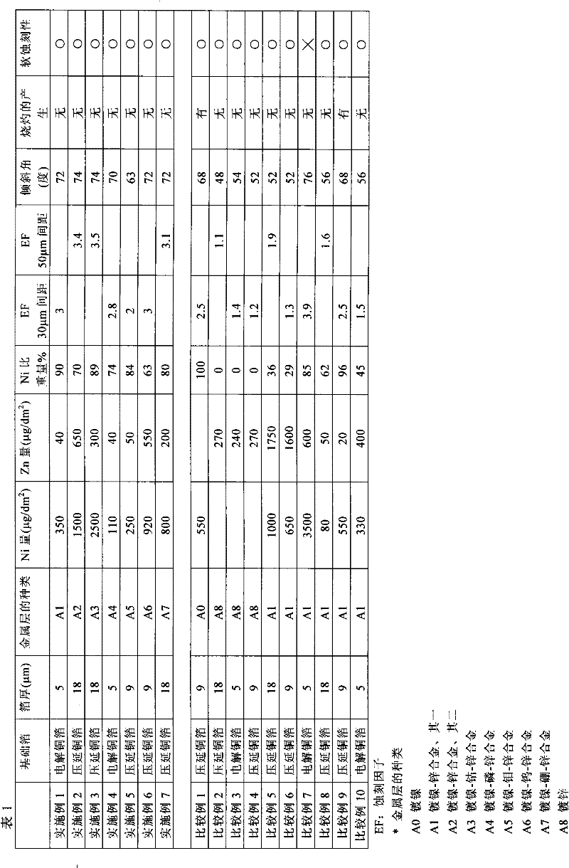
[0196] At this time, as shown in Table 1, the nickel content in the nickel-zinc alloy coating is 350 μg / dm 2 , the zinc content is 40μg / dm 2 . The nickel ratio is 90% by weight. The copper foil was bonded to the resin substrate using the side opposite to the surface provided with the nickel-zinc alloy plating layer as an adhesive surface.

[0197] Then, 10 circuits were printed through resist coating and exposure steps, and an etching process for removing unnecessary portions of the copper foil was performed. The etching conditions, circuit formation conditions, measurement conditions of etching factor, and burning test are as follows.

[0198] (etching conditions)

[...

Embodiment 2

[0220] A rolled copper foil with a foil thickness of 18 μm was used. The surface roughness Rz of this rolled copper foil was 0.7 micrometers. Under the conditions of the above-mentioned nickel-zinc alloy plating (Part 2), 2150 μg / dm was formed on the rolled copper foil 2 nickel-zinc alloy coating. As shown in Table 1, the amount of nickel in the nickel-zinc alloy coating is 1500 μg / dm 2 , the amount of zinc is 650μg / dm 2 . At this time, the nickel ratio was 70% by weight.

[0221] In addition, the copper foil was bonded to the resin substrate with the side opposite to the surface provided with the nickel-zinc alloy plating layer as an adhesive surface.

[0222] Then, 10 circuits were printed through the resist coating and exposure process similarly to Example 1, and the etching process for removing unnecessary part of copper foil was given.

[0223] Except for the circuit formation conditions, the etching conditions, the measurement conditions of the etching factor, and ...

Embodiment 3

[0232] A rolled copper foil with a foil thickness of 18 μm was used. The surface roughness Rz of this rolled copper foil was 0.7 micrometers. Under the above nickel-cobalt-zinc alloy plating conditions, a nickel-cobalt-zinc alloy plating layer is formed on the rolled copper foil. At this time, the cobalt substitution amount was 8% of the nickel amount (% by weight) in terms of nickel.

[0233] As shown in Table 1, the nickel content in the nickel-cobalt-zinc alloy coating is 2500 μg / dm 2 , the zinc content is 300μg / dm 2 . At this time, the nickel ratio was 89% by weight. In addition, this nickel ratio is the nickel equivalent amount of the total amount of cobalt and nickel.

[0234] In addition, the copper foil was bonded to the resin substrate using the side opposite to the surface provided with the nickel-cobalt-zinc alloy plating layer as an adhesive surface.

[0235] Then, 10 circuits were printed through the resist coating and exposure process similarly to Example 1...


PUM

PropertyMeasurementUnit
surface roughnessaaaaaaaaaa
widthaaaaaaaaaa
surface roughnessaaaaaaaaaa

Abstract

The present invention provides a rolled copper foil or an electrolytic copper foil for an electronic circuit, wherein the circuit is formed by etching, wherein the rolled copper foil or electrolytic copper foil has a nickel alloy layer formed on the etched side with a lower etching rate than copper , the nickel alloy layer contains zinc. The subject of the present invention is that, when forming a circuit by etching the copper foil of a copper-clad laminate, it is possible to prevent the downward bending caused by etching, to form a circuit with a uniform width of the target circuit, and to shorten the circuit formation time by etching as much as possible. Time, and the thickness of the nickel alloy layer can be reduced as much as possible, and oxidation can be suppressed when heated, and discoloration commonly known as "burning" can be prevented, and etchability in pattern etching can be improved, and short circuit or poor circuit width can be prevented.

Description

technical field [0001] The present invention relates to a rolled copper foil or an electrolytic copper foil for an electronic circuit that forms a circuit by etching, and to a method of forming an electronic circuit using the same. Background technique [0002] Copper foils for printed circuits are widely used in electronic and electrical equipment. Copper foils for printed circuits are generally bonded to substrates such as synthetic resin boards or films with adhesives or without adhesives under high temperature and high pressure to produce copper clad. Afterwards, in order to form the target circuit, the circuit is printed through resist coating and exposure processes, and after etching treatment to remove unnecessary parts of the copper foil, various components are soldered, thereby forming an electronic device. printed circuit. [0003] Copper foils used in such printed circuits are roughly classified into electrolytic copper foils and rolled copper foils depending on ...

Claims


Application Information

Patent Timeline
Patent Type & Authority Applications(China)
IPC IPC(8): C25D7/06B32B15/01C23F1/02H05K1/09
CPCC25D5/12C25D7/0614B32B15/01C25D5/48H05K3/384H05K2201/0355H05K3/067C23C22/24H05K2203/0723C23F1/02C23F1/18C23F1/28H05K3/06C25D3/562H05K2201/0338Y10T428/12229Y10T428/31678C25D7/06H05K1/09
Inventor 山西敬亮神永贤吾福地亮
Owner JX NIPPON MINING & METALS CORP
Learn More